Understanding the Impact of Ion Migration on PCB Reliability
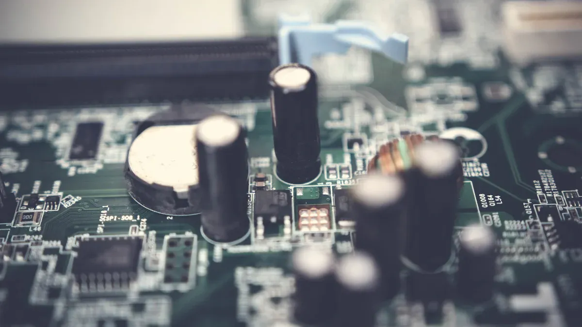
Ion migration causes up to 25% of pcb failure, damaging printed circuit boards and reducing long-term reliability. Engineers, designers, and manufacturers must understand ionic contamination, as ionic substances in pcb materials often trigger dendrite growth and corrosion. The table below highlights why controlling ionic contamination matters in pcb production.
Aspect | Description | Relevance to Engineers, Designers, and Manufacturers |
|---|---|---|
Ion Migration Mechanism | Ion migration in semiconductors is mediated by defects and impurities, affecting electronic, optical, and mechanical properties. | Understanding these mechanisms is critical for improving device performance and reliability. |
Computational Methods | Use of density functional theory (DFT), molecular dynamics (MD), and machine learning (ML) to predict defect formation energies, migration pathways, and energy barriers. | Enables accelerated materials discovery and design by predicting ion migration behavior, reducing experimental costs and time. |
Experimental Techniques | Techniques like secondary ion mass spectrometry (SIMS) and deep-level transient spectroscopy (DLTS) provide diffusion profiles but have limitations in resolution and cost. | Complement computational methods to validate models and provide practical insights into ion diffusion in devices. |
Materials Studied | Focus on photovoltaic materials such as metal halide perovskites and CdTe, which are promising for solar cells due to efficiency and cost. | Knowledge of ion migration in these materials helps improve stability, efficiency, and manufacturability of semiconductor devices. |
Impact on Device Performance | Ion migration influences device stability, efficiency, and long-term reliability. | Controlling ion migration is essential for engineers and manufacturers to produce durable and high-performance semiconductor devices. |
Integration of ML and DFT | ML models trained on DFT data accelerate prediction of defect behavior and ion migration, enabling screening of materials with suppressed ion migration. | Facilitates design of novel semiconductors with desired properties, aiding designers and manufacturers in material selection and process optimization. |
Key Takeaways
Ion migration causes up to 25% of PCB failures by promoting corrosion and dendrite growth, which can lead to short circuits and reduce long-term reliability.
Regular testing using methods like ROSE and Ion Chromatography helps detect ionic contamination early, allowing manufacturers to control risks and improve PCB quality.
Choosing advanced materials, following strict cleaning protocols, and applying smart design guidelines significantly reduce ionic contamination and extend PCB lifespan.
Ion Migration Basics

What Is Ion Migration
Ion migration describes the movement of charged particles, known as ions, within materials. In the context of pcb manufacturing, this process involves ionic species traveling across the surfaces or through the layers of printed circuit boards. Ionic movement can occur when moisture is present, creating a pathway for these particles. This phenomenon often leads to reliability issues in pcb assemblies. Engineers recognize that ion migration can cause corrosion, dendrite growth, and even short circuits. The Nernst-Planck transport equation models this process, showing how ions diffuse and migrate within the thin moisture film that forms on pcb surfaces. Electrochemical impedance spectroscopy helps measure the resistance and concentration of these ions, providing insight into the risk of failure. The presence of ionic contaminants, such as residues from manufacturing, increases the likelihood of ion migration and subsequent pcb degradation.
How Ion Migration Happens
Ion migration in pcb materials follows a series of steps:
Moisture forms a thin film on the surface of printed circuit boards, often due to environmental humidity.
Anodic metal ion dissolution begins, where metals like tin or copper release ions through electrochemical reactions.
These metal ions migrate through the moisture film, driven by an electric field between conductors.
At the cathode, metal ions deposit and form dendrites, which can grow and eventually bridge gaps between conductors.
Laboratory tests, such as the Water Drop Test and Thermal Humidity Bias Test, confirm these mechanisms. For example, scanning electron microscopy reveals that tin and copper ions migrate and deposit as dendrites, especially under high humidity. The presence of ionic residues accelerates this process. Over time, these dendrites can cause short circuits, leading to pcb failure. Outdoor exposure studies also show that corrosion and ion migration occur in real-world conditions, with nickel and other metals migrating outward and forming visible corrosion products. These findings highlight the importance of controlling ionic contamination during pcb manufacturing to ensure long-term reliability.
Causes in PCB Manufacturing
Ionic Contaminants
Ionic contamination stands as a leading cause of pcb failure. During fabrication and assembly, residues from flux, handling, and incomplete cleaning introduce unwanted ionic species onto pcb surfaces. These contaminants include anions such as chloride, bromide, nitrate, and sulfate. Ion chromatography studies reveal that specific ion concentrations directly correlate with failure mechanisms like dendrite formation and short circuits. Statistical analysis shows that ionic contamination accounts for about 25% of pcb failures.
Manufacturers use two main testing methods to measure ionic contamination. The ROSE test provides a quick assessment of total ionic contamination but does not identify specific ions. Ion Chromatography (IC) testing delivers detailed data on individual ionic species and their concentrations. IC results relate contamination to surface area, allowing precise contamination control and failure analysis.
Units of Measurement | Typical Values / Limits | Description / Notes | |
|---|---|---|---|
ROSE Test | micrograms (ug) or milligrams (mg) NaCl per square inch or cm² | Fail point: 10.06 ug NaCl/sq inch (IPC standard) | Measures ionic contamination by resistivity of solvent extract; uses 75% isopropanol + 25% water solvent. |
Ion Chromatography | mg/cm² equivalent NaCl | Permitted contamination: <0.0001 mg/cm² (bare boards), ~0.0003 mg/cm² (hand-soldered assemblies) | Identifies specific ionic species (e.g., sodium formate, chloride, bromide, nitrate, sulfate). |
Conductivity/Resistivity | Converted to NaCl equivalents | N/A | Conductivity increases with ionic contamination; used to calculate NaCl equivalent contamination. |
These quantitative measurements help manufacturers monitor contamination quality and ensure pcb reliability by detecting ionic residues from fabrication and assembly. LT CIRCUIT uses advanced materials and strict process controls to minimize ionic contamination, supporting high reliability in every pcb.
Environmental Factors
Environmental conditions play a significant role in the introduction and movement of ionic contamination on pcb assemblies. High humidity, temperature fluctuations, and airborne pollutants increase the risk of ionic migration. Moisture forms a thin film on pcb surfaces, creating a pathway for ionic species to move between conductors. This movement leads to corrosion, dendrite growth, and eventual short circuits.
Accelerated stress testing, such as high temperature and humidity exposure, reveals how environmental factors influence ionic migration. Studies show that copper ion migration increases under these conditions, especially when air is present in the test chamber. These findings highlight the importance of environmental controls and robust contamination control measures during pcb manufacturing and storage. LT CIRCUIT implements environmental monitoring and advanced testing to ensure that each pcb meets strict reliability standards.
Substrate and Solder Mask
The choice of substrate and solder mask materials directly affects the level of ionic contamination and the risk of ion migration. Halogen-free laminates and advanced resin systems provide superior moisture resistance and stable resin structures. These materials reduce electrochemical migration, such as conductive anodic filament (CAF) formation. High-quality glass fabric with proper thickness and surface treatment enhances resin adhesion and mechanical stability, further mitigating ionic migration.
Design optimizations, including larger conductor and via spacing and staggered via layouts, increase the physical distance and complexity of ionic migration paths. Manufacturing process controls, such as improved drilling quality and controlled lamination, reduce voids and defects that can initiate ion migration.
LT CIRCUIT selects advanced substrates and solder masks to minimize ionic contamination and enhance pcb reliability. The brand’s commitment to contamination control ensures that each pcb resists the effects of ionic contamination, even in demanding environments.
The effects of ionic contamination can be severe, but with proper material selection and process control, manufacturers can significantly reduce the risk. LT CIRCUIT’s use of innovative materials and strict contamination control practices sets a high standard for pcb reliability.
Reliability Impact
Electrochemical Migration
Electrochemical migration stands as a major threat to pcb reliability. This process begins when ionic contaminants, such as chloride or sulfate, remain on the pcb surface after manufacturing. When moisture is present, these ionic substances dissolve and form a conductive path between metal traces. An electric field across the pcb drives the movement of these ions, causing metal atoms to dissolve at the anode and redeposit at the cathode. Over time, this leads to the formation of conductive filaments that can bridge gaps between conductors.
Laboratories use several advanced techniques to study electrochemical migration on pcb materials:
3D confocal microscopy and environmental scanning electron microscopy help observe changes in surface morphology.
Energy-dispersive X-ray spectroscopy and Raman spectroscopy analyze the composition of corrosion products.
Scanning Kelvin probe measures changes in surface potential, revealing corrosion states.
Electrochemical impedance spectroscopy evaluates how corrosion affects the electrical properties of capacitors.
Direct observation of dendrite formation and growth between electrodes provides insight into the physical effects of ionic contamination.
These assessments give engineers a clear picture of how electrochemical migration damages pcb assemblies. They show that ionic contamination can quickly lead to corrosion and loss of long-term reliability.
Note: Electrochemical migration does not only cause visible damage. It also changes the electrical properties of the pcb, making failures harder to detect until they become severe.
Dendrite Growth and Shorts
Dendrite growth represents one of the most dangerous outcomes of ionic contamination on pcb surfaces. Dendrites are tiny, tree-like structures that form when metal ions move through a thin film of moisture and deposit onto the cathode. As these dendrites grow, they can eventually connect two conductors that should remain isolated.
The process of dendrite formation follows these steps:
Ionic contaminants dissolve in surface moisture.
An electric field causes metal ions to migrate from the anode to the cathode.
Metal ions deposit and form dendrites, which extend toward the opposite conductor.
When dendrites bridge the gap, they create a conductive path, leading to short circuits.
Engineers often use microscopic imaging to monitor dendrite growth on pcb assemblies. These observations reveal that dendrite formation can happen rapidly under high humidity and voltage stress. Once a dendrite bridges two conductors, the pcb may experience sudden failure. This type of failure can be catastrophic, especially in safety-critical applications.
A table below summarizes the key risks associated with dendrite growth:
Risk Factor | Impact on PCB Reliability |
|---|---|
High ionic contamination | Increases dendrite formation rate |
Elevated humidity | Accelerates dendrite growth |
Small conductor spacing | Raises risk of short circuits |
Inadequate cleaning | Leaves ionic residues behind |
Dendrite growth highlights the importance of controlling ionic contamination during pcb manufacturing. Even small amounts of ionic residue can trigger rapid failure, reducing the long-term reliability of the device.
Long-Term Degradation
Long-term degradation of pcb assemblies often results from ongoing ionic contamination and electrochemical migration. Over months or years, repeated exposure to moisture and environmental stress causes metal corrosion, insulation breakdown, and gradual loss of performance. Studies show that ion migration under high humidity leads to failures in electronic components, directly reducing the life expectancy of pcbs.
Experts explain that ionic contamination speeds up failure mechanisms such as metal corrosion and electrochemical migration. This acceleration means that pcbs with high ionic residue degrade much faster than clean boards. Early testing for ionic contamination helps manufacturers detect and address these risks before products reach the field.
Research combining accelerated degradation testing and real-world data shows that environmental factors like temperature, humidity, and airborne salts all promote ion migration. These conditions shorten the lifespan of pcbs by increasing the rate of corrosion and electrical failure. Detailed failure analyses of electronic devices confirm that ion migration leads to changes in current response, defect formation, and rapid performance loss.
Technical reports provide further insight:
Real-time microscopic imaging shows visible changes in pcb materials as ions move under an electric field.
Activation energy calculations confirm that ion migration occurs at room temperature, making it a constant risk.
Transmission electron microscopy links ion migration to loss of crystal structure in pcb materials.
Changes in current-voltage characteristics and photoluminescence spectra demonstrate rapid degradation caused by ionic movement.
Engineers and manufacturers must prioritize contamination control and regular testing to protect the long-term reliability of pcb assemblies. By understanding and managing ionic contamination, they can extend product life and reduce costly failures.
Detection and Testing
ROSE and IC Methods
Regular ionic contamination testing is essential for maintaining pcb reliability. The ROSE (Resistivity of Solvent Extract) test and Ion Chromatography (IC) stand as the most widely used methods for detecting ionic contamination on pcb surfaces. The ROSE test, standardized under IPC-TM-650 Method 2.3.25, measures the total ionic residue by extracting contaminants with a solvent and checking resistivity. This method, referenced in IPC-J-STD-001 and MIL-STD-2000, sets clear limits for acceptable ionic contamination and helps manufacturers control ion migration risks. IC provides detailed identification of specific ionic species, allowing for precise ionic contamination testing and targeted process improvements.
Standard / Method | Description / Role in Testing ROSE and IC Methods |
|---|---|
IPC-TM-650 Method 2.3.25 | Documents the ROSE test procedure for detecting ionic contamination on PCBs. |
IPC-J-STD-001 | Specifies acceptable ionic contamination limits for high-reliability electronics. |
MIL-STD-2000 | Military standard referenced for ionic cleanliness requirements, including ROSE test limits. |
LT CIRCUIT uses both ROSE and IC methods as part of its advanced ionic contamination testing protocols, ensuring every pcb meets strict industry standards.
SIR Testing
Surface Insulation Resistance (SIR) testing evaluates how ionic contamination affects the electrical insulation between conductors on a pcb. IPC-TM-650 Method 2.6.3.7 defines this test, which applies voltage across test patterns under controlled humidity and temperature. SIR testing detects drops in insulation resistance caused by ionic migration, dendrite growth, or conductive anodic filament formation. This method provides early warning of potential failures, making it a key part of ionic contamination testing for high-reliability pcb assemblies.
Accelerated Life Tests
Accelerated life tests, such as Highly Accelerated Stress Test (HAST) and Electromigration & SIR tests, predict long-term pcb reliability under ionic contamination stress. HAST exposes pcbs to high temperature, humidity, and pressure, rapidly accelerating failure mechanisms linked to ionic migration. Electromigration & SIR tests apply bias voltage under harsh conditions, continuously monitoring insulation resistance. These tests correlate accelerated outcomes with real-world performance, confirming that effective ionic contamination testing leads to longer-lasting pcb products.
Regular ionic contamination testing protects pcb assemblies from hidden risks. LT CIRCUIT ensures quality by using advanced testing services and strict adherence to industry standards, delivering reliable pcbs for demanding applications.
Prevention and Best Practices
Cleaning and Handling
Proper cleaning and handling remain essential for reducing ionic contamination on pcb assemblies. Many industries have shown that effective cleaning protocols prevent ion migration. For example, environmental engineers at a former Air Force base used regenerable ion exchange resins and careful regeneration procedures to control ion migration of contaminants. In art conservation, experts learned that specific cleaning treatments and layer combinations in oil paintings reduce vulnerability to ionic migration, preserving durability. Membrane system operators found that cleaning with NaOH restored ion transport and prevented fouling, which can obstruct ionic movement. These examples show that thorough cleaning and careful handling protect pcb surfaces from ionic residues, supporting long-term reliability.
Material Choices
Selecting the right materials helps minimize ionic contamination in pcb manufacturing. High-quality laminates and advanced solder masks resist moisture and block ionic movement. LT CIRCUIT uses innovative substrates and solder masks that lower the risk of ion migration. These choices support best practices for minimizing ionic contamination and ensure that each pcb meets the demands of high-reliability electronics.
Design Guidelines
Engineers follow specific design guidelines to reduce ionic contamination and prevent ion migration. They increase spacing between conductors, use staggered via layouts, and avoid sharp corners. These steps make it harder for ionic species to travel across the pcb. LT CIRCUIT applies these best practices for minimizing ionic contamination in every design, helping customers achieve reliable performance.
Industry Standards
Industry standards set clear requirements for controlling ionic contamination in pcb production. Standards like IPC-J-STD-001 and IPC-TM-650 guide manufacturers in testing and process control. LT CIRCUIT aligns its processes with these standards, using advanced testing and strict quality checks. This commitment ensures that every pcb meets or exceeds industry expectations for reliability and safety.
LT CIRCUIT leads the industry by combining advanced materials, strict process controls, and adherence to standards. This approach protects pcb assemblies from ionic contamination and supports long-term success.
Ion migration causes major reliability issues in pcb assemblies.
Surface roughness increases nine times, and ionic contamination speeds up pcb failure.
Voltage, electrode spacing, and chloride ion levels change pcb short circuit times.
LT CIRCUIT uses advanced manufacturing, testing, and prevention to protect pcb products from ionic threats.
Engineers should choose best practices and partner with reliable pcb manufacturers to reduce ionic risks and extend pcb life.
FAQ
What is the main cause of ion migration in electronic assemblies?
Ionic contamination from residues left during manufacturing often triggers ion migration. Moisture on surfaces allows ions to move, which can lead to reliability issues.
How can manufacturers detect ionic contamination?
Manufacturers use tests like ROSE and Ion Chromatography. These methods help identify and measure ionic residues that may cause problems in electronic assemblies.
Why is controlling ion migration important for reliability?
Ion migration can create shorts and corrosion. Preventing it helps electronic assemblies last longer and perform better in demanding environments.
See Also
Typical Challenges And Fixes In PCB Design For SMT
How LDI Technology Affects The Quality Of PCB Manufacturing
Tin Immersion Effects On PCB Surface Finish And Mask Stability
Enhancing Signal Integrity Through Impedance Control In PCB Production
VCP Application’s Role In Achieving Uniform Copper Thickness In PCBs