What knowledge should be mastered for PCB multi-layer circuit board layout
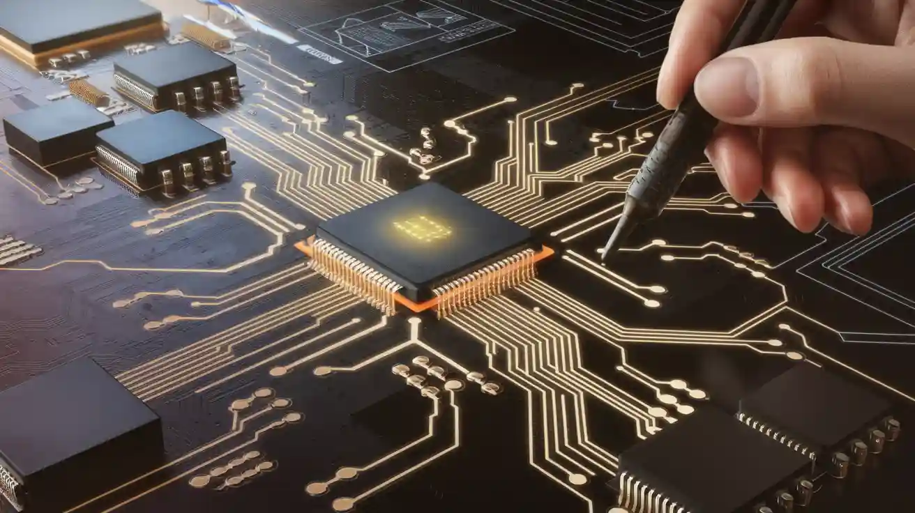
Mastering multi-layer PCB layout is important for making good electronics, as it requires knowledge mastered in various key areas. It helps products work well and fit modern technology needs. Small size and high performance are very important today. A good PCB lasts longer, costs less, and gains user trust. Industries like phones, healthcare, and cars use multi-layer PCBs a lot, showcasing how essential they are in electronics now. Key skills like handling heat, controlling signals, and fast routing are needed. These skills keep signals strong and stop problems like overheating. Learning this helps you make PCBs that work great in tough situations.
Key Takeaways
Learning multi-layer PCB design makes products work better and last longer. Focus on skills like handling heat and keeping signals clear.
Pick the right layer setup for your PCB. A good setup lowers noise and makes signals better.
Good grounding and power layers are very important. They keep things steady and cut down on interference.
Use design tools early to check for problems. These tools can spot issues like too much heat or bad signals before making the PCB.
Follow rules and standards for PCB design. This keeps your PCB safe, easy to make, and high quality.
Basics of Multi-Layer PCB Design
Understanding Layer Stack-Up
Layer stack-up is how layers are arranged in a PCB. It includes conductive and insulating layers. A good stack-up makes the PCB work better and last longer. For example, a 4-layer PCB has a signal layer, ground plane, power plane, and another signal layer. This setup reduces noise and keeps signals clear.
More complex designs need more layers. An 8-layer PCB separates signal layers with power and ground planes. This lowers electromagnetic interference (EMI) and keeps signals strong. A 10-layer PCB is great for fast signals. It pairs signal and return planes closely, improving performance.
Layer Count | Configuration Description | Key Benefits |
|---|---|---|
4 Layers | Signal-Ground-Power-Signal | Reduces noise, crosstalk, and improves signal return |
6 Layers | Top signal, ground, inner signal, power, ground, bottom signal | Better EMI control and stronger signals |
8 Layers | Signal separated by power and ground planes | Less crosstalk, better signal quality |
Picking the right stack-up is very important. It helps the PCB handle fast signals, avoid interference, and keep signals clear.
Importance of Grounding and Power Planes
Grounding and power planes are key in multi-layer PCBs. Ground planes give signals a stable reference and reduce noise. They also provide a low-impedance path for return currents. This is crucial for fast designs where signal quality matters.
Power planes supply power to parts of the PCB. They prevent voltage drops and improve performance. Placing power and ground planes next to each other reduces EMI and boosts signal quality.
Plan these planes carefully for the best results. For instance, putting a ground plane under a signal layer gives a clear return path. This lowers the chance of signal problems. Using multiple ground planes in fast designs also reduces crosstalk and improves shielding.
Material Selection for Multi-Layer PCBs
The materials used in a PCB affect how well it works. Problems like material outgassing, temperature changes, and vibrations can be solved with the right materials.
Challenge | Description | Mitigation Strategies |
|---|---|---|
Material Outgassing | Release of gases in low-pressure environments affecting parts. | Use low outgassing materials like Polyimide and PTFE, or protective coatings. |
Extreme Temperature Fluctuations | Big temperature changes causing stress and damage. | Use materials with matching CTE and thermal vias for heat spread. |
Vibration and Mechanical Stresses | Vibrations causing physical damage to the PCB. | Choose strong materials and designs for better stability. |
Radiation Effects | Damage from radiation exposure. | Use radiation-resistant materials and shielding. |
Common materials include FR4, Polyimide, and PTFE. FR4 is cheap and good for general use. Polyimide handles heat well, making it great for hot environments. PTFE is good for high-frequency designs because it has low dielectric loss.
When picking materials, think about thermal conductivity, dielectric constant, and CTE. Matching the CTE of materials and parts prevents damage from heat stress.
Tip: Always check with your PCB maker to ensure the materials fit your design and meet standards.
Component Placement Strategies
Thermal Management Considerations
Good thermal management keeps your PCB working well. Too much heat can damage parts and shorten their life. To fix this, add airflow paths, heat sinks, or thermal vias. For example, put hot components near heat sinks or airflow paths to cool them faster.
Thermal tools like FloTHERM help you see heat spread on your PCB. These tools show hot spots and let you fix them before building the PCB. Tools like T3Ster check how well your cooling methods work. Using through-silicon vias improves heat control, helping your PCB handle high temperatures better.
Tip: Start using thermal tools early to avoid fixing costly mistakes later.
Ensuring Signal Integrity During Placement
Signal quality depends on where parts are placed and traces are routed. Keep high-speed parts close together to make traces shorter. Shorter traces lower resistance and reduce noise. Ground planes also help by giving a steady reference and cutting down interference.
Studies show that placing parts smartly improves signal quality. For example:
Evidence | Explanation |
|---|---|
Better placement improves signal quality | Shorter traces and ground planes reduce noise. |
Short traces lower parasitic effects | Long traces cause more resistance and noise. |
Double-sided PCBs allow direct routing | Easier paths keep signals strong. |
Plan your layout carefully to keep signals strong and your PCB reliable.
Power Distribution and Decoupling Capacitors
Good power distribution stops voltage drops and keeps parts stable. Place decoupling capacitors near power pins to filter noise and steady voltage. Group capacitors near fast parts to stop power changes and improve performance.
Placing power and ground planes close together also helps. This lowers impedance and cuts down electromagnetic interference. It ensures all parts get steady power.
Note: Use simulation tools to check power flow and fix problems early.
Routing Techniques for Multi-Layer PCBs
Differential Pair Routing
Differential pair routing is key for fast designs. It uses two signal traces placed close together. These traces carry opposite currents, canceling out EMI. This method keeps signals clean and reduces noise. It works well for data communication and fast processors.
Differential pairs also keep signals strong. Their design lowers crosstalk, which happens in single-ended signals. They handle quick signal changes better, making them great for high-speed channels. Keeping the traces evenly spaced ensures steady impedance. This reduces signal reflections and keeps signals clear.
Parameter | Description |
|---|---|
Signal Reflections | Happen when impedance is not consistent. |
Crosstalk | Signals interfering with each other, lowering quality. |
Signal Attenuation | Signal strength loss along the path. |
Jitter | Timing changes that affect performance. |
Signal to Noise Ratio Degradation | Noise makes it hard to detect correct signals. |
Over- and Undershoot | Signal distortions causing wrong logic readings. |
Increased Radiated Emission | More emissions needing extra shielding for compliance. |
Tip: Keep differential pairs close and spacing even for best results.
Impedance Control and Signal Path Optimization
Impedance control is vital for good signals in multi-layer PCBs. Signals face impedance based on trace width, spacing, and material. If impedance doesn’t match, signals reflect and lose quality.
To improve signal paths, match trace lengths and widths. Proper spacing keeps impedance steady, reducing noise. Tools like Time Domain Reflectometry (TDR) check impedance. TDR sends pulses through the PCB to find mismatches.
Benefits of Impedance Control:
Cuts down EMI.
Reduces signal reflections and noise.
Boosts system reliability and performance.
Matches source and load impedance for better power transfer.
Note: Adjust trace width, layers, and materials to get correct impedance.
Via Placement and Minimization of Crosstalk
Vias connect layers in multi-layer PCBs but need careful placement. Badly placed vias can delay signals and cause crosstalk. Crosstalk happens when signals interfere, lowering quality and causing problems.
To avoid crosstalk, space signal traces apart and don’t route them parallel for long. Use ground planes to shield traces and cut interference. Limit vias in fast signal paths to keep signals strong. Each via adds inductance and capacitance, which can hurt signal quality.
Measured Benefits of Proper Routing:
Better circuit performance with fewer delays.
More reliable power distribution.
Less interference, keeping signals clear.
Tip: Use simulation tools to check crosstalk and plan via placement before finishing your design.
Design Rules and Checks
Clearance and Creepage Requirements
Clearance and creepage distances are important for PCB safety. Clearance is the shortest air gap between two conductive parts. Creepage is the shortest path along an insulating surface. Both stop electrical sparks and keep insulation working well.
To follow these rules, check voltage levels and safety standards early. For example, IPC-2221 gives rules for clearance and creepage based on material and voltage. Tools like NEXTRA can check your design for problems automatically.
Source | Description |
|---|---|
IPC-2221 | Gives rules for material quality and layout for clearance and creepage. |
NEXTRA | Software that finds design issues in electro-mechanical assemblies. |
Trace Spacing Guide | Explains how voltage affects PCB design. |
Tip: Think about humidity and dirt, as they can change creepage distances.
Manufacturability and DFM (Design for Manufacturing)
DFM makes sure your PCB can be built easily and without mistakes. Following DFM rules avoids problems like broken vias, shorts, and bad signals. It also saves time and lowers costs.
Important DFM checks include copper spacing, drill sizes, and thermal patterns. For instance, too much copper can cause overheating. Small spacing can lead to signal interference. A DFM checklist helps ensure your design is ready for production.
Key Aspect | Importance |
|---|---|
Design for Manufacturability (DFM) | Stops problems like broken vias and electrical shorts. |
IPC Standards | Makes sure designs meet industry rules for reliability. |
DFM Checklist | Includes copper spacing, drill sizes, and thermal patterns. |
Placing parts smartly and routing traces well makes manufacturing easier. This leads to better, cheaper, and more reliable products.
Ensuring Compliance with Industry Standards
Following industry standards ensures your PCB meets quality and safety rules. Standards like IPC-2221 and IPC-A-610 guide layout, materials, and visual checks. ISO certifications, like ISO 9001, are needed for selling worldwide.
Standard | Description |
|---|---|
ISO 9001 | Focuses on quality systems to meet customer and legal needs. |
IPC-2221 | Gives general PCB design rules. |
UL 94V-0 | Makes sure PCBs meet fire safety rules. |
RoHS | Limits harmful materials like lead and mercury. |
Note: Following these rules makes your designs safer, eco-friendly, and accepted globally.
By using these design rules, you can make PCBs that are safe, easy to build, and meet industry standards. This reduces risks and improves your product’s success.
Advanced Techniques for Multi-Layer PCB Layout
High-Speed Routing Best Practices
High-speed routing needs careful planning to keep signals clear. Keep traces short to avoid delays and reflections. Shorter traces help signals move faster and stay strong. Use controlled impedance routing to match the source and load. This stops signals from weakening or losing quality.
Differential pair routing is very useful. Place the two traces close together and make them the same length. This keeps signals balanced and reduces EMI. Avoid sharp turns in traces, as they can cause problems. Use smooth curves or 45-degree angles for better results.
Tip: Tools like Time Domain Reflectometry (TDR) check impedance and improve trace design.
EMI Reduction Techniques
Lowering EMI helps your PCB work well in noisy places. Separate analog and digital grounds to stop noise from mixing. Place parts wisely, keeping sensitive ones away from noisy areas.
Ferrite beads block high-frequency noise on power and signal lines. Shielded cables protect against outside EMI, and special PCB materials reduce interference inside the board. Thicker copper traces improve current flow and cut down resistive losses, lowering EMI further.
Ways to Reduce EMI:
Use differential pair routing for fast signals.
Keep analog and digital grounds apart.
Place parts carefully to avoid noise.
Add ferrite beads and shielded cables.
Use high-frequency materials and thicker copper.
Note: Blind and buried vias also help reduce EMI exposure.
Using Simulation Tools for Validation
Simulation tools find and fix problems before making the PCB. Parasitic extraction tools check for unwanted effects like capacitance and inductance. Network simulations test signal strength by including these effects. EMI simulations check for interference to meet standards.
Thermal simulations show where heat builds up and how it moves. Computational Fluid Dynamics (CFD) simulations show airflow, helping with cooling. Mechanical simulations test for vibration and stress, ensuring the PCB stays strong.
Purpose | |
|---|---|
Parasitic extraction | Finds unwanted effects in the layout. |
Network simulations | Tests signal strength with parasitics included. |
EMI simulations | Checks for electromagnetic interference. |
Thermal simulations | Shows heat buildup and movement. |
CFD simulations | Displays airflow for better cooling. |
Mechanical simulations | Tests for vibration and physical stress. |
Tip: Start using these tools early to save time and money.
Common Mistakes to Avoid
Skipping Thermal Management
Not managing heat can cause big problems in your PCB. Too much heat can break parts and shorten your product’s life. Plan ways to remove heat to avoid these issues. Use tools like thermal vias, heat sinks, and airflow paths to cool your PCB.
Bad heat design often leads to more failures. For example:
Circuits with parts too close together fail more often.
About 35% of failures happen because of poor cooling.
Packed circuits can fail one after another due to heat buildup.
To stop these problems, space parts well and use thermal tools. These tools show hot spots and help fix designs before making the PCB. Always focus on heat management to keep your PCB working well.
Forgetting Signal Integrity
Signal problems can hurt how your PCB works. Fast signals are easily affected by noise, reflections, and crosstalk. Good routing and grounding are needed to keep signals strong.
Place fast parts close to each other to make traces short. Shorter traces lower noise and resistance. Ground planes give signals a steady base and reduce interference. Differential pair routing is also helpful. It cancels out EMI and keeps signals clear.
Ignoring signal quality can cause errors, lost data, and system crashes. Use simulation tools to find and fix problems early. These tools improve your design and make your PCB more reliable.
Incomplete Manufacturing Documents
Bad or missing documents can cause problems during production. This can lead to mistakes, delays, and higher costs. Clear and detailed files are needed for smooth manufacturing.
Important files include:
Gerber Files: Show details about each PCB layer.
Drill Files: Ensure correct hole sizes and placement.
Fabrication Drawings: Explain the PCB’s size and technical details.
Quality Requirements: List checks to meet standards.
Without good documents, manufacturers may face problems like solder issues or misaligned parts. These mistakes can weaken your PCB and hurt your reputation. Good documentation ensures your PCB is made correctly and works well.
Tip: Double-check your documents before sending them to the manufacturer. This step avoids mistakes and saves money.
Tools and Software Recommendations
Popular PCB Design Software Options
Picking the right PCB design software is very important. It helps you create better layouts and work faster. Many tools make designing easier and more accurate. Below is a table showing popular software and their user ratings:
Software | User Rating |
|---|---|
Altium Designer | 4.5/5 |
Cadence Allegro | 4.6/5 |
Mentor Graphics Xpedition | 4.4/5 |
OrCAD PCB Designer | 4.3/5 |
Zuken CR-8000 | 4.5/5 |
Pulsonix PCB Design | 4.2/5 |
Autodesk EAGLE | 4.1/5 |
PADS Professional | 4.3/5 |
SolidWorks PCB | 4.5/5 |
KiCAD | 4.6/5 |
EasyEDA | 4.4/5 |
Fritzing | 4.0/5 |
CircuitMaker | 4.3/5 |
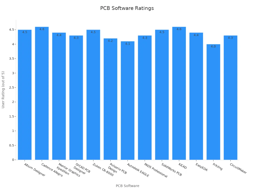
If you’re just starting, try KiCAD or EasyEDA. They are free and simple to use. For more advanced features, Altium Designer and Cadence Allegro are great options. These tools help you design faster and make high-quality PCBs.
Simulation and Analysis Tools
Simulation tools are very helpful for checking your PCB design. They show problems like signal issues, overheating, or weak spots before building the PCB. Simulations make sure your design works well in real life.
Here are some common simulation types:
DC Voltage Drop Simulation: Checks if parts get enough power.
Electro-Thermal Simulation: Finds overheating problems.
Thermal-Mechanical Simulation: Tests if the PCB stays strong under heat.
For fast designs, signal integrity analysis is very important. It finds issues like noise or signal reflections. To get good results, match your settings to real-world conditions.
Tip: Use tools like HyperLynx or Ansys SIwave for signal checks. They give detailed feedback on your design.
Resources for Learning and Skill Development
To get better at PCB design, use good learning resources. Online courses, forums, and books can teach you new skills and keep you updated. Here are some helpful options:
Online Courses: Websites like Coursera and Udemy offer lessons for all levels.
Community Forums: Sites like PCBWay and Stack Exchange answer design questions.
Books: Try "PCB Design for Beginners" or "High-Speed Digital Design" for deeper learning.
Simulation Tutorials: Many tools, like Altium and KiCAD, have free guides to help you.
Note: Practice often and join design challenges to improve your skills and confidence.
Knowledge Mastered with LT CIRCUIT
LT CIRCUIT’s Skill in Multi-Layer PCB Design
LT CIRCUIT is a top expert in multi-layer PCB design. They have years of experience making high-quality PCBs for industries like cars, phones, and electronics. Their team knows how to handle complex designs, including layer setups, grounding, and heat control. This ensures your PCBs meet high standards for performance and reliability.
They also use advanced methods to create detailed designs. If you need HDI PCBs or boards with many layers, they can help. Their focus on accuracy and new ideas ensures your projects turn out great.
How LT CIRCUIT Keeps Signals Strong and Reliable
Good signal quality is very important for PCBs, especially fast ones. LT CIRCUIT uses smart techniques to keep signals clear. They carefully route traces, control impedance, and reduce crosstalk. These steps make sure signals stay strong and avoid interference.
They also use simulation tools to check designs before making them. These tools find problems like signal reflections or EMI early. Fixing these issues ensures your PCBs work well, even in tough conditions.
Advanced PCB Options from LT CIRCUIT
LT CIRCUIT offers many advanced PCB options for modern needs. They make HDI PCBs, multi-layer boards, and high-frequency designs. You can customize features like solder mask colors and finishes such as ENIG or HASL.
They test every PCB carefully to ensure quality. Tests like flying probe and E-tests check if the boards meet your needs. With LT CIRCUIT, you get advanced solutions that improve your devices’ performance and durability.
Tip: Check out LT CIRCUIT’s products to see how they can improve your PCB designs.
Understanding how to design multi-layer PCBs needs key skills. These include managing heat, reducing noise, and making designs easy to build. Each skill helps your PCB work well and follow industry rules. The table below explains these important areas:
Knowledge Area | Description |
|---|---|
Heat management | Stops parts from overheating and keeps the board lasting longer. |
Reducing noise (EMI) | Cuts down signal problems by smart routing and grounding. |
Easy manufacturing (DFM) | Makes sure designs are simple and affordable to produce. |
Design rule checks (DRC) | Finds and fixes mistakes by following design rules. |
Teamwork and communication | Helps teams share ideas and solve design problems early. |
Using LT CIRCUIT’s knowledge, you can make better PCBs. Their tools and methods make designing easier, so you can focus on creating new ideas. Try their tips and explore their services to improve your PCB designs.
FAQ
What is the main advantage of using multi-layer PCBs?
Multi-layer PCBs save space by stacking layers together. This helps create smaller, faster devices. They also keep signals clear and reduce EMI, making them great for gadgets like phones and medical tools.
How do you choose the right materials for multi-layer PCBs?
Pick materials based on heat, strength, and electrical needs. For general use, choose FR4. Use Polyimide for hot areas and PTFE for fast signals. Always check with your PCB maker to ensure the materials work well.
Why is grounding important in multi-layer PCB design?
Grounding gives signals a steady base and cuts noise. It also lowers EMI and crosstalk, keeping your PCB reliable. A good ground plane improves signal strength and protects against interference.
What tools can help you ensure signal integrity?
Use tools like HyperLynx and Ansys SIwave to check signals. These tools find problems like noise or reflections. Fixing these issues early makes your design better before production.
How does LT CIRCUIT support advanced PCB designs?
LT CIRCUIT is skilled in making multi-layer PCBs. They ensure strong signals and reliable boards. They offer advanced options like HDI and high-speed PCBs. They also test designs to meet your needs. Visit LT CIRCUIT for more info.
Tip: Use simulation tools to check your design and avoid mistakes.
See Also
Understanding Multilayer PCBs and Their Impact on Electronics
Explore Cutting-Edge HDI PCB Prototyping Methods Right Now
Utilizing Horizontal Copper Sinking Technology in PCB Manufacturing