How Multilayer PCBs Are Made: A Detailed Process Overview
You start making a multilayer pcb by following a detailed manufacturing process. Each step, from design to testing, shapes the quality and reliability of your printed circuit boards. LT CIRCUIT leads the industry in multilayer pcb manufacturing. The company uses advanced equipment and strict standards to deliver top results.
Metric / Specification
Value / Description
Multilayer PCB Layers
4 to 32 layers
PCB Thickness Range
0.2 mm to 6.0 mm
Certifications
ISO 9001, ISO 14001
Customer Testimonials
Signify (Philips) USA, SpaceX
The manufacturing process of multilayer pcbs involves many stages. Each stage supports the strength and performance of your multilayer pcbs. When you look for multilayer pcb manufacturing, LT CIRCUIT stands out for its experience and innovation in pcb manufacturing. With over 400 employees and more than 5,000,000 pcbs produced each year, you can trust LT CIRCUIT for your next multilayer pcb manufacture. Making a pcb with LT CIRCUIT ensures you receive high-quality multilayer pcbs every time.
Key Takeaways
Multilayer PCB manufacturing involves careful design, precise layer stacking, and strict quality control to ensure strong, reliable circuit boards.
Advanced technologies like Laser Direct Imaging, Automated Optical Inspection, and precise drilling help create accurate, high-performance multilayer PCBs.
Choosing the right materials, surface finishes, and thorough testing guarantees your multilayer PCB meets your product’s needs for durability and performance.
Design & Data Preparation
File Review
You begin the manufacturing process of multilayer pcbs by reviewing your design files. Careful file review helps you avoid common mistakes that can affect your multilayer pcb. When you check your files, you look for missing layers, misaligned drill files, and incorrect scaling. These errors can cause delays, extra costs, and even defects in your pcbs.
Missing layers can weaken your multilayer board.
Misaligned drill files may lead to holes in the wrong places.
Incorrect scaling can make your pcb the wrong size.
If you do not catch these problems early, you might need extra design reviews, which add 10-15% more time to your project. Each time you fix a data flaw, you add 1-2 weeks to your schedule. More prototype builds and higher costs can follow. Careful data preparation keeps your multilayer pcb project on track and helps you avoid field failures.
Stack-Up Planning
Stack-up planning shapes the structure of your multilayer pcb. You decide how to arrange the layers, copper, and insulation. Good stack-up planning keeps your pcb flat and strong. It also helps control electromagnetic interference and signal quality.
You want symmetry in copper distribution and layer arrangement. This prevents bow and twist in your multilayer pcbs. You also keep signal, ground, and power planes in the right order to reduce noise. Keeping minimum distances between planes and avoiding adjacent signal layers supports quality.
Parameter | Statistical Measure / Tolerance |
|---|---|
Controlled impedance tolerance | ±10% |
Layer-to-layer registration | Up to 50µm (1.9685 mil) |
Board thickness (less than 15 mil) | ±2 mil |
Board thickness (15 to 31 mil) | ±3 mil |
Board thickness (31 mil and above) | ±10% |
These tolerances help you maintain signal integrity and prevent warping in your multilayer pcb. Careful stack-up planning is a key part of the manufacturing process of multilayer pcbs.
Inner Layer Production
Imaging
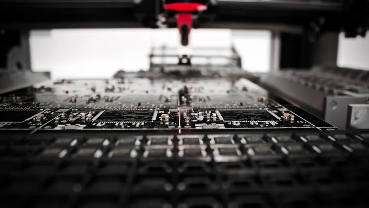
You start the inner layer production by transferring your multilayer pcb design onto copper-clad laminates. This step uses advanced imaging techniques to create precise patterns for each layer. You apply a photosensitive dry film to the copper surface. Then, you expose the film to ultraviolet light through a photomask that matches your circuit design. The exposed areas harden, while the unexposed parts remain soft and get washed away.
Modern imaging systems, such as Direct Imaging (DI) and Laser Direct Imaging (LDI), use high-precision lasers to expose the photoresist. These technologies help you achieve finer features and better alignment between layers. Automated Optical Inspection (AOI) systems check for defects like shorts, opens, or incorrect feature sizes. You benefit from:
High-resolution cameras that detect even tiny defects.
Electrical testing methods that verify copper trace connections.
Cross-sectional analysis to check copper thickness and etching quality.
Statistical Process Control (SPC) to reduce variation and improve consistency.
These steps ensure your multilayer pcb meets strict quality standards during the manufacturing process.
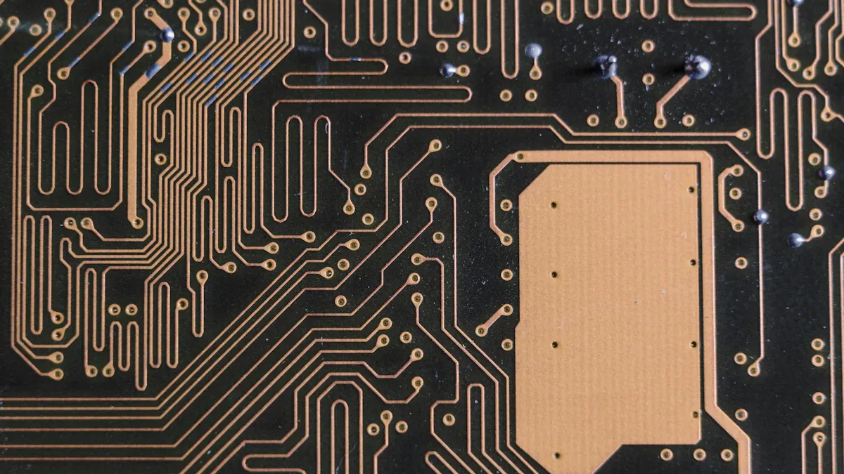
Etching
After imaging, you move to the etching stage. Here, you remove unwanted copper from the inner layers, leaving only the circuit paths you need. The etching process uses a chemical solution in a clean room to prevent contamination. You control the etchant composition, temperature, and etch rate to achieve precise results.
Parameter | Specification | Control Methodology |
|---|---|---|
Etchant Composition | CuCl₂/HCl/H₂O₂ (2.8N) | Automated titrator dosing |
Temperature Control | 50±0.3℃ | RTD cascade system |
Etch Rate | 2.1±0.15 μm/min | In-line XRF thickness mapping |
Undercut Control | <12% of trace width | Cross-sectional SEM analysis |
You finish by removing the dry film resist, revealing the copper circuitry. AOI checks the etched layers against digital images to catch any defects. This careful process ensures each multilayer pcb layer is accurate and reliable, supporting the overall manufacturing process of multilayer pcbs.
Layer Alignment & Lamination
Layer Stacking
You start the next step in the manufacturing process by stacking the layers of your multilayer pcb. Each layer must line up perfectly to make sure your board works as designed. For multilayer boards with six or more layers, you use rivets to hold the inner layers together. This stops the layers from shifting. When you need even more precision, you use the PIN LAM method. This method uses special pins to keep every layer in the exact position.
Before you stack the layers, you check each one with Automated Optical Inspection (AOI) technology. AOI finds any defects and makes sure the graphics on each layer are correct. You also use registration punching to drill precise alignment holes in every layer. This step helps you keep strict alignment during the multi-layer lamination process. Many factories use automation in the LayUp step to reduce mistakes and improve accuracy.
Rivets fix inner layers for stability.
PIN LAM method gives exact alignment.
AOI checks for defects before stacking.
Registration punching drills alignment holes.
Lamination Process
You move to the lamination process after stacking the layers. You place the stacked layers into a press. The press uses heat and pressure to bond the layers into one solid board. This step is critical in the manufacturing process of multilayer pcbs. The multi-layer lamination process melts the resin in the prepreg sheets, which then flows and fills any gaps between layers.
Quality control plays a big role here. You use slicing tests to check the thickness of the insulation between layers. Thermal shock tests help you find any weak spots that could cause the layers to separate. Copper foil adhesion tests make sure the copper stays attached to the board. These tests help you make sure your multilayer pcb is strong and reliable.
Drilling & Via Formation
Drilling
You start this stage of the manufacturing process by drilling holes through your copper multilayer pcb. These holes, called vias, connect the different layers inside your board. You can use mechanical drilling for standard multilayer boards or laser drilling for microvias in high-density designs. Each method offers different accuracy and hole sizes.
Metric | Description | Typical Tolerance / Notes |
|---|---|---|
Hole Position Accuracy | Difference between designed and drilled hole center | ±0.05 mm |
Hole Diameter | Actual hole size vs. specified size | ±0.025 mm |
Circularity | Roundness of hole, ratio of max/min diameters | Close to 1 indicates high circularity |
Barrel Hole Wall | Taper or hourglass shape of plated hole due to plating thickness variation | Affects hole resistance |
Hole Breakout | Separation around hole exit on outer layer | Affects pad connection quality |
Drill Smear | Resin debris on hole wall after drilling | Impacts copper plating adhesion and conductivity |
You need to control drill bit wear and spindle stability to keep your copper multilayer pcb accurate. Using positioning pins and regular equipment checks helps you avoid misalignment. Baking the board before drilling can also reduce shrinkage and improve results. For copper multilayer pcb designs with very small holes, laser drilling gives you higher accuracy and less thermal impact.
Copper Plating
After drilling, you move to copper plating. This step coats the inside of each via with a thin layer of copper, making electrical connections between layers in your copper multilayer pcb. You use electroless copper plating to start, which deposits copper evenly inside every hole. The typical copper thickness for vias in a copper multilayer pcb is about 25 to 35 microns.
You check the quality of the plating with X-ray inspection and thermal cycling tests. Most copper multilayer pcb vias pass these tests, with a 98.5% pass rate in sample batches. Minor voids appear in only a small number of vias, and misalignment stays within safe limits. You can trust this process to give you strong, reliable connections for your multilayer pcb assembly.
Tip: Careful copper plating ensures your copper multilayer pcb will last longer and perform better in demanding applications.
Outer Layer Manufacturing Process
Imaging
You start the outer layer process by imaging the top and bottom layers of your multilayer pcb. LT CIRCUIT uses advanced Laser Direct Imaging (LDI) technology for this step. LDI gives you higher resolution and accuracy than traditional photomasks. You can create fine-pitch traces and complex patterns that modern electronics need. LDI supports line widths and spaces as small as 25 microns. This helps you build dense and miniaturized boards.
LDI uses computer-aided positioning and fiducial marks for better alignment.
The process removes the need for physical photomasks, which reduces defects from contamination.
LDI allows for quick design changes and faster prototyping.
The method also cuts down on material waste and chemical use, making the manufacturing process cleaner.
Automated Optical Inspection (AOI) checks the imaged layers for defects like opens, shorts, or pattern errors. Manual inspection alone cannot catch every problem. AOI improves detection accuracy and keeps your production consistent.
Etching
After imaging, you move to etching. This step removes unwanted copper, leaving only the circuit paths you need. LT CIRCUIT controls the etching process with high precision. You check for etch back, undercut, and overcut to make sure the copper features match your design. You also measure copper thickness and conductor width to keep circuit dimensions exact.
AOI and manual checks find defects such as shorts, opens, and spacing issues.
Registration accuracy stays within a few microns, which is critical for multilayer alignment.
Surface cleanliness inspections prevent bonding problems and improve reliability.
LT CIRCUIT monitors etchant solutions to ensure consistent etch quality.
You rely on these advanced techniques to manufacture outer layers that meet strict quality standards. Precision in imaging and etching supports the overall reliability of your multilayer pcb.
Solder Mask & Legend
Solder Mask Application
You protect your multilayer PCB with a solder mask. This green (or sometimes other color) layer covers the board and leaves only the pads and vias exposed. The solder mask keeps solder from bridging between traces during assembly. It also shields copper from moisture, dust, and chemicals.
You apply the solder mask using a screen printing or spray process. After application, you cure the mask with heat or ultraviolet light. LT CIRCUIT uses automated equipment to ensure even coverage and precise alignment. You want the solder mask to stick well and last a long time. Industry standards like IPC-SM-840 and IPC-6012 set the rules for solder mask quality. These standards define how hard the mask should be, how well it sticks, and how it resists heat and chemicals.
You can check solder mask quality with several tests:
Adhesion testing, such as the cross-hatch and tape peel tests, checks if the mask peels off.
Coverage testing uses Automated Optical Inspection (AOI) and UV light to find thin spots or defects.
Thickness control ensures the mask is between 20-30 microns for best protection.
These steps help you get a reliable, high-quality finish on your multilayer PCB.
Legend Printing
You add the legend, or silkscreen, after the solder mask cures. The legend shows part numbers, symbols, and reference designators. You print it using inkjet or screen printing. Good legend printing helps you identify components and makes assembly easier. LT CIRCUIT uses high-contrast, durable inks that resist smudging and fading. You get clear, readable markings that last through the life of your board.
Tip: A well-applied solder mask and clear legend make your PCB easier to assemble and maintain.
Surface Finishing
ENIG, HASL, and More
You protect your multilayer PCB with a surface finish. This finish covers the exposed copper pads and helps you get strong solder joints during assembly. It also keeps the copper from oxidizing or corroding over time. You can choose from several types of finishes, each with its own strengths.
Surface Finish | Solderability | Corrosion Resistance | Shelf Life | Best Use Cases | |
|---|---|---|---|---|---|
HASL | Low | Good | Moderate | Moderate (~12 mo) | Through-hole, budget electronics |
ENIG | Moderate | Excellent | Excellent | Long (up to 24 mo) | Fine-pitch, high-reliability, harsh settings |
OSP | Low | Good | Moderate | Short (~6 mo) | High-volume, less critical boards |
Immersion Silver | Moderate | Excellent | Moderate | Moderate (~12 mo) | High-frequency, lead-free assembly |
ENEPIG | High | Excellent | Excellent | Long (up to 24 mo) | Wire bonding, mixed assembly, premium boards |
ENIG (Electroless Nickel Immersion Gold) gives you a flat, smooth surface. You get excellent solderability and strong corrosion resistance. ENIG works best for fine-pitch parts and high-reliability products like smartphones, aerospace, and medical devices. The gold layer keeps your board stable even in tough conditions. ENIG costs more but lasts longer and supports advanced designs.
HASL (Hot Air Solder Leveling) is a popular, cost-effective choice. You get good solder joints, especially for through-hole parts. HASL works well for less demanding products. The surface is not as flat as ENIG, so it is less suited for tiny components. HASL also has a shorter shelf life.
Other finishes like OSP, Immersion Silver, and ENEPIG offer more options. OSP is eco-friendly and cheap but does not last as long. Immersion Silver supports high-frequency signals. ENEPIG gives you a very flat surface and works for wire bonding.
Tip: Choose your surface finish based on your product’s needs. For high-reliability and fine-pitch designs, ENIG is often the best choice. For cost savings, HASL or OSP may work well.
Profiling & Cutting
Routing
You shape your multilayer PCB by routing. Routing means cutting the board outline and any special shapes you need. You use computer-controlled machines called CNC routers. These machines follow your design files with high accuracy. You can create straight edges, curves, and even slots for connectors.
You want every cut to be clean and precise. LT CIRCUIT uses advanced CAD tools and simulation software to plan each route. Automated test equipment, like network analyzers and time-domain reflectometers, checks the board during fabrication. These tools help you keep the right impedance and signal speed.
You also benefit from strong process control. LT CIRCUIT uses:
Statistical process control (SPC) to spot and fix any problems fast.
In-process inspections and electrical tests to catch defects early.
Specialized equipment that keeps copper trace widths and spacing exact.
Continuous improvement programs to keep machines running at their best.
Note: Careful routing helps your board fit perfectly in its case and keeps all signals working as designed.
Board Separation
You finish the process with board separation. This step removes each PCB from the larger manufacturing panel. You can use routing, v-scoring, or punching, depending on your board’s shape and size.
Routing cuts around each board, leaving small tabs. You break these tabs to free the board. V-scoring makes shallow grooves so you can snap boards apart. Punching works best for simple shapes and high-volume runs.
Separation Method | Best For | Edge Quality | Speed |
|---|---|---|---|
Routing | Complex shapes | Smooth | Moderate |
V-Scoring | Straight edges | Good | Fast |
Punching | Simple, high volume | Fair | Very Fast |
You check each board for smooth edges and correct size. LT CIRCUIT’s careful process ensures your multilayer PCB is ready for assembly and use.
Quality Control in Multilayer PCB Manufacturing
Quality control stands at the heart of multilayer pcb manufacturing. You want every board to work perfectly, so you need strong checks at every step. LT CIRCUIT uses advanced tools and strict standards to make sure your boards meet the highest quality. You benefit from a process that combines technology, skilled people, and proven methods.
Electrical Testing
You rely on electrical testing to catch problems before your multilayer PCB leaves the factory. These tests check if your board works as designed and can handle real-world use. LT CIRCUIT uses several types of electrical tests to make sure your board is safe and reliable:
Continuity tests check for open circuits and shorts by sending a small current through each trace.
Hi-pot tests apply high voltage to see if the insulation between circuits holds up, which is important for high-voltage boards.
In-circuit testing (ICT) uses custom fixtures to measure voltage and current at test points. This test finds bad solder joints, missing parts, and wrong values.
Flying probe tests use moving probes to touch different points on your board. This method finds faults without needing a custom fixture, which is great for prototypes or small batches.
Time domain reflectometry (TDR) checks signal integrity and impedance, which matters for high-speed designs.
ROSE tests measure if any solder flux residue remains, which could cause problems later.
Stress tests, like vibration and thermal shock, show if your board can survive tough conditions.
You get results like pass/fail, resistance values, and voltage readings. LT CIRCUIT documents these results and compares them to your requirements. This process helps you avoid costly failures in the field.
Tip: LT CIRCUIT follows industry standards like UL, ISO, IPC, and RoHS. You can trust that your multilayer pcb manufacturing meets global safety and quality rules.
Visual Inspection
Visual inspection gives you another layer of protection in multilayer pcb manufacturing. Skilled inspectors and automated machines look for surface and hidden defects. LT CIRCUIT uses Automated Optical Inspection (AOI) and X-ray inspection to spot problems that eyes might miss.
AOI scans the board for missing parts, wrong placements, and solder issues.
X-ray inspection checks inside the board for hidden defects, such as voids in solder joints or misaligned layers.
Certified inspectors do final checks to make sure every board looks right and matches your design.
You also benefit from process controls like Statistical Process Control (SPC) and Pareto analysis. These methods help LT CIRCUIT find and fix problems early, which means fewer mistakes and better boards for you.
Quality Benchmark / Process Efficiency Metric | Description | Demonstrated Outcome |
|---|---|---|
Early detection and reduction of defects during production | Reduced mistakes and improved PCB quality reliability | |
Automated Optical Inspection (AOI) & X-ray Inspection | Advanced inspection methods to identify surface and hidden defects | Faster defect detection, 40% defect reduction in some cases |
AI-driven Models & Digital Twin Technology | Use of AI to optimize machine performance and predict issues | 40% faster product launch, 99.8% first-pass yield |
Compliance with Industry Standards | Following material, design, manufacturing, and testing rules | Guarantees safety, reliability, and legal compliance |
You see the results in the numbers. LT CIRCUIT achieves a 98% positive evaluation score before shipping. This high score shows that the quality control system works well and that you get reliable boards every time.
Note: LT CIRCUIT uses test point design rules to make testing easier and more reliable. This is especially important for automotive and healthcare PCBs, where safety matters most.
You can trust LT CIRCUIT’s multilayer pcb manufacturing process to deliver boards that meet your needs for quality, safety, and performance.
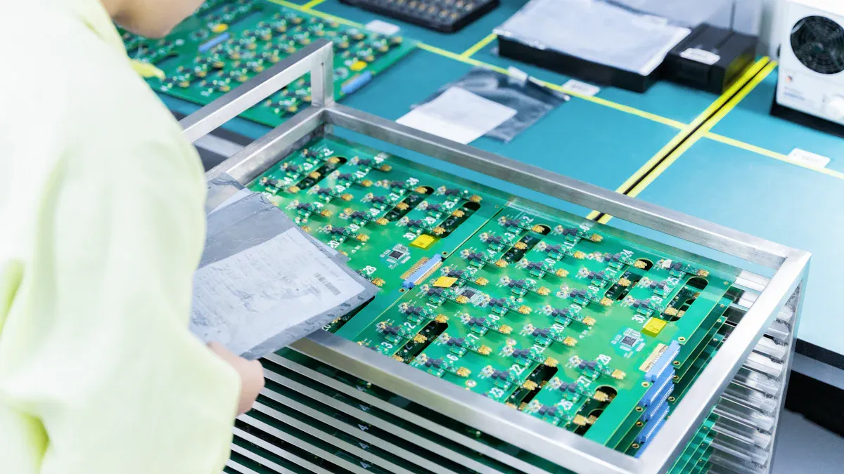
Packaging by LT CIRCUIT
Cleaning
You want your multilayer PCB to arrive clean and ready for assembly. LT CIRCUIT uses advanced cleaning methods to remove any dust, flux, or residues left from manufacturing. You benefit from water-based, non-foaming solvents that clean powerfully and dry without leaving residues. These solvents work well for both small and large production runs.
You see several steps in the cleaning process:
High-purity, lint-free pre-saturated wipes remove particles and oils from the board surface.
Stencil wiping papers with long, strong fibers scrub away stubborn residues and improve cleaning quality.
Online or offline cleaning machines replace manual cleaning, giving you higher consistency and better results.
You avoid problems like white residues, which can come from polymerized rosin or unreacted activators. These residues affect the appearance and may cause reliability issues. LT CIRCUIT uses mixed solvents—both polar and non-polar—to dissolve these residues effectively. Cleaning happens soon after assembly to prevent hardening and corrosion. After cleaning, the boards dry in a controlled environment to keep them spotless.
Tip: Proper cleaning helps your PCB meet industry standards and ensures long-term performance.
Final Packing
You receive your PCBs in packaging designed to protect them from damage and contamination. LT CIRCUIT uses anti-static bags to shield your boards from static electricity. You also get moisture barrier bags for extra protection against humidity.
You find each board separated by soft, lint-free sheets to prevent scratches. Strong outer cartons keep your shipment safe during transport. Labels on each package show product details and traceability codes, making inventory easy for you.
You can trust LT CIRCUIT’s packaging process to deliver your multilayer PCBs in perfect condition, ready for your next step.
You follow each step in multilayer PCB manufacturing to achieve reliable results. Every stage matters for quality. LT CIRCUIT uses advanced machines, real-time monitoring, and strict testing to ensure high performance. Review these key metrics:
Metric | Focus Area |
|---|---|
ORE | Resource use |
OEE | Equipment use |
Trust LT CIRCUIT for dependable multilayer PCB solutions.
FAQ
What is the main advantage of multilayer PCBs?
You get more circuits in a smaller space. Multilayer PCBs help you build compact, powerful devices like smartphones, computers, and medical equipment.
How do you ensure the quality of each PCB?
You benefit from strict inspections, electrical tests, and automated checks. LT CIRCUIT uses advanced tools to catch defects before shipping your boards.
Can you customize the number of layers in your PCB?
Yes, you can choose the number of layers based on your project needs. LT CIRCUIT offers multilayer PCBs from 4 up to 32 layers.
See Also
A Comprehensive Guide To The PCB Fabrication Process
Step-By-Step Production Of Multilayer Rigid-Flex Boards
Understanding The Complete Process Of PCB Manufacturing
Advanced Production Techniques For Heavy Copper Multilayer PCBs
Challenges And Processes In Multi-Layer Circuit Board Prototyping