How to Minimize Current Noise During Circuit Board Manufacturing
Minimizing current noise is essential for circuit board reliability. You can boost performance by optimizing component placement and shortening trace lengths. Noise disrupts signal characteristics, especially in high-frequency circuits. Electromagnetic interference lowers signal integrity and can cause faulty operation. During the production process, you should use strategies like separating analog and digital sections, placing decoupling capacitors close to ICs, and avoiding long parallel traces.
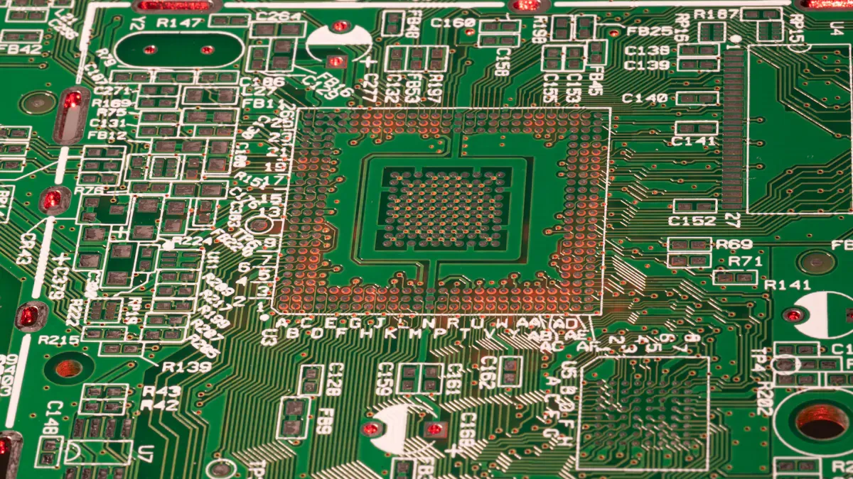
Layer stackup and strategic component placement help reduce electromagnetic interference.
Preferred | Not Recommended |
|---|---|
Single capacitor value | |
Isolated digital and analog ground | Single ground net |
Guard fence around board edge | No fence or poor edge clearance |
Key Takeaways
Optimize your layer stack-up by placing solid ground and power planes in the middle. This reduces noise and improves signal integrity.
Use multiple decoupling capacitors near active devices to filter out high-frequency noise and stabilize power supply.
Maintain proper trace spacing to prevent crosstalk and electromagnetic interference, ensuring better signal quality.
Minimize loop area by keeping signal traces short and routing them over continuous ground planes to reduce current noise.
Separate analog and digital components on your circuit board to protect sensitive signals from digital switching noise.
Key Noise Reduction Strategies
Optimize Layer Stack-Up
You can reduce current noise by planning the layer stack-up of your circuit board. Place solid ground and power planes in the middle of the stack. This lowers loop inductance and shields signals from electromagnetic interference. Keep high-speed signal layers close to ground planes. This gives signals a stable return path and improves impedance control. Separate high-speed and low-speed signals to prevent crosstalk. Use stripline or microstrip configurations for routing. These methods help balance signal integrity and manufacturing efficiency.
Tip: Avoid routing high-speed traces over splits in the ground plane. This prevents signal distortion and keeps noise low.
Layer Type | |
|---|---|
1 | Top Signal (High-Speed Signals) |
2 | Ground Plane |
3 | Signal Layer (High-Speed) |
4 | Ground Plane |
5 | Power Plane (e.g., 3.3V) |
6 | Signal Layer (Mixed Signals) |
7 | Ground Plane |
8 | Signal Layer (Mixed Signals) |
9 | Signal Layer (Mixed Signals) |
10 | Ground Plane |
11 | Signal Layer (Mixed Signals) |
12 | Power Plane (e.g., 5V) |
13 | Ground Plane |
14 | Signal Layer (High-Speed) |
15 | Ground Plane |
16 | Bottom Signal (High-Speed) |
A well-designed stack-up shields against radiation and reduces noise coupling during the production process.
Use Continuous Ground Planes
You should dedicate an entire layer to a continuous ground plane. This provides a consistent return path for signals and lowers loop inductance. Place ground vias close to signal transitions. This keeps the loop area small and reduces electromagnetic interference. Avoid routing signals over gaps in the ground plane. Gaps increase noise and cause signal distortion.
Note: Continuous ground planes improve immunity to external radiation and enhance signal integrity.
Place Decoupling Capacitors Properly
Decoupling capacitors play a key role in minimizing current noise. Select capacitor values based on the transient current needs of your devices. Use 0.01 µF to 0.1 µF capacitors for high-frequency decoupling. Larger capacitors, such as 10 µF or 100 µF, stabilize the power supply for low-frequency transients. Place several capacitors near each active device. This compensates for parasitic inductance and keeps the current loop area small. Mount capacitors as close as possible to power and ground planes. Avoid routing traces between the capacitor pad and the via. This lowers inductance and improves high-frequency performance.
Tip: Use capacitors with a higher self-resonant frequency to filter out high-frequency noise.
Maintain Trace Spacing
Proper trace spacing prevents crosstalk between adjacent traces. You should keep traces apart to reduce coupling and maintain signal quality. Adequate spacing also helps block electromagnetic interference from external sources. This improves the signal-to-noise ratio and keeps your circuit board reliable.
Crosstalk prevention
Noise reduction
Improved signal quality
Control Impedance Routing
Impedance control is essential for signal integrity. You need to maintain consistent impedance along signal paths. This reduces electromagnetic interference and signal loss. Use proper routing techniques, such as keeping differential pairs symmetrical and referencing solid ground planes. These steps help you avoid noise issues and keep signals stable throughout the production process.
Minimize Loop Area
You can lower current noise by minimizing the loop area of current paths. Keep signal traces short and route them over continuous ground planes. Place decoupling capacitors close to IC power pins, within 2 mm if possible. Use via stitching to connect ground planes, spacing vias at wavelength/20 intervals. Arrange power and ground vias in alternating pairs instead of grouping power vias together. These actions reduce electromagnetic radiation and improve signal integrity.
Callout: A smaller loop area cuts down on radiated emissions and makes your circuit board less susceptible to noise.
Current Noise Basics
What Is Current Noise?
You encounter current noise when unwanted electrical signals disrupt the flow of current in your circuit board. These disturbances often come from rapid switching, fluctuating power supplies, or electromagnetic fields. Current noise can appear as random spikes or irregular patterns in your circuit. You may notice it as interference that affects how your board performs. When you design or manufacture a PCB, you must recognize that current noise can travel through traces, ground planes, and even the air around your board.
Tip: You can reduce current noise by keeping signal paths short and using proper grounding techniques.
Why It Matters for PCBs
Current noise affects your PCB in several ways. You may see problems like ground bounce, crosstalk, and electromagnetic interference. These issues can cause your circuit to malfunction or lose signal quality.
Ground bounce happens when signals fail to return to the ground reference quickly. This creates unexpected current spikes and may lead to circuit errors.
Crosstalk occurs when signals from one trace influence another. Insufficient spacing between traces increases this risk and lowers signal integrity.
Electromagnetic interference (EMI) results from poor ground return paths. Irregular signal paths generate interference and noise, which can disrupt your board’s operation.
Effect | Impact on PCB Functionality |
|---|---|
Ground Bounce | Causes current spikes and malfunctions |
Crosstalk | Leads to signal integrity issues |
EMI | Generates interference and noise |
You must control current noise to ensure your PCB works reliably. If you ignore noise, your board may fail in critical applications. By understanding current noise, you can apply strategies that protect your circuit and improve performance.
Main Noise Sources in PCB Production
Electromagnetic Interference (EMI)
You face electromagnetic interference when electronic devices generate unwanted electromagnetic noise. EMI can disrupt the operation of your circuit board and nearby equipment. During the production process, you encounter EMI from both human-made and natural sources. High-frequency oscillators, switching power supplies, motors, and wireless communication devices often produce EMI. Device layout, wiring quality, and grounding methods also play a role.
High-frequency oscillators
Switching power supplies
Motors
Wireless communication devices
Device layout
Wiring quality
Grounding methods
Tip: You can reduce EMI by improving grounding and shielding in your circuit board design.
Crosstalk Between Traces
Crosstalk happens when signals from one trace interfere with another. You see this effect because of capacitive and inductive coupling between traces. This coupling leads to unwanted signals on adjacent traces and can cause signal degradation. Malfunctions in critical circuits may result from crosstalk. Factors such as trace spacing, return path design, and the presence of vias can make the noise worse.
Capacitive and inductive coupling between traces
Signal degradation and malfunctions
Trace spacing, return path, and vias increase noise
Callout: Keep traces apart and use proper return paths to minimize crosstalk.
Power Supply Fluctuations
You must pay attention to power supply fluctuations during PCB manufacturing. These fluctuations introduce current noise and affect sensitive components. Ripple, transients, and ground loops are common types of power supply noise. Each type impacts circuit performance in different ways.
Type of Power Supply Noise | Description | Impact on OCXO Performance |
|---|---|---|
Ripple | Residual AC components in DC supplies | Can induce frequency deviations up to ±0.1 ppm |
Transients | Sudden spikes from load switching or EMI | Increases phase noise by 3–5 dB at 1 kHz offset |
Ground Loops | Current imbalances introducing noise | Disrupts temperature control, causing ±0.05 ppm frequency drift |
Note: Stable power supplies help you maintain signal integrity throughout the production process.
Layout and Placement Issues
You can increase current noise if you overlook layout and placement. Stray magnetic fields from parallel currents and ground returns may induce unwanted offsets in sensor output. Improper sensor placement near high-current paths leads to measurement errors and reduced accuracy. Inadequate ground plane management creates uniform bias fields that shift the sensor's null point, introducing nonlinearity.
Stray magnetic field interference
Improper sensor placement near high-current paths
Inadequate ground plane management
Tip: Careful layout and placement decisions help you avoid noise and improve circuit accuracy.
Noise Control in the Production Process
Prevent Cold Solder Joints
Cold solder joints can create unwanted resistance and increase current noise on your circuit board. You can prevent these issues by following a few important steps during the production process:
Clean all components and surfaces with a solvent to remove dirt and oil.
Use high-quality soldering tools for better control and reliability.
Pre-heat your soldering iron and keep it at least 15°C above the solder alloy’s melting point.
Apply enough solder to make a strong connection, but avoid using too much.
Maintain a stable environment free from vibrations while soldering.
Control the temperature to ensure the solder melts and flows properly.
Tip: Careful soldering helps you avoid weak joints that can act as noise sources in your finished board.
Ensure Quality Assembly
You improve signal integrity and reduce noise by focusing on quality assembly throughout the production process. When you follow proper assembly standards, you prevent problems like cold solder joints and loose connections. These issues can cause noise spikes and disrupt signals, especially in high-speed circuits. Careful assembly and thorough inspections help you build reliable boards that perform well in demanding environments.
Inspect for Noise Issues
Inspection is a key step in controlling noise during the production process. You should check every board for visible defects, such as poor solder joints or misplaced components. Use magnification tools to spot small cracks or gaps in solder connections. Electrical testing can help you find hidden noise sources that visual checks might miss. If you find any problems, fix them before moving to the next stage.
Inspection Step | What to Look For |
|---|---|
Visual Inspection | Cold solder joints, misalignment |
Magnification Check | Cracks, gaps, or weak joints |
Electrical Testing | Unexpected resistance or noise |
Callout: Early detection and correction of noise issues save time and improve the overall quality of your circuit boards.
Practical Tips for Implementation
Material Selection
You can improve your circuit board’s noise performance by choosing the right materials. Start with a continuous ground plane. This lowers impedance and blocks unwanted signals. Use via stitching to connect ground planes. Multiple vias reduce inductance and boost shielding. Fill unused board areas with copper. This copper pour increases current capacity and keeps your board stable. Thicker copper, such as 2 oz, helps carry higher currents and lowers resistance. Make your ground plane as large as possible. A bigger ground area means lower impedance and better noise control. Always divide ground domains with care. This prevents floating islands that can cause noise.
Technique/Material | Description |
|---|---|
Ground Plane | A continuous ground plane reduces impedance and minimizes noise. |
Via Stitching | Using multiple vias to connect ground planes reduces inductance and improves shielding. |
Ground Fill (Copper Pour) | Filling unused areas with copper increases current capacity and stability, essential for noise reduction. |
Copper Thickness | Using thicker copper (2 oz) for high currents can reduce resistance, aiding in noise minimization. |
Plane Sizing | A larger ground plane area provides lower impedance, crucial for effective noise management. |
Divide with Purpose | Properly managing ground domains prevents floating islands that can cause noise issues. |
Tip: Select materials that match your design’s current and frequency needs for the best results.
Zone Separation for Analog and Digital
You should separate analog and digital zones on your circuit board. Place analog circuits away from digital ones. This keeps digital switching noise from reaching sensitive analog signals. Use separate ground planes for each zone when possible. Connect these planes at a single point to avoid ground loops. Route analog and digital traces on different layers. This reduces the chance of crosstalk. Mark each zone clearly during the production process. This helps assembly teams avoid mistakes and keeps noise low.
Place analog and digital components in different areas
Use separate ground planes with a single connection point
Route traces on different layers
Callout: Clear zone separation protects your analog signals from digital noise.
Testing and Verification
You need to test your circuit boards before final use. Use oscilloscopes to check for unwanted noise on power and signal lines. Measure impedance and look for spikes or irregular patterns. Test boards under real operating conditions. This shows how noise behaves during the production process. Inspect solder joints and component placement. Small defects can create big noise problems. Keep a checklist for each test. This ensures you do not miss any steps.
Use oscilloscopes for noise checks
Measure impedance and signal quality
Test under real conditions
Inspect assembly quality
Note: Careful testing and verification help you catch noise issues early and improve board reliability.
You can achieve reliable circuit boards by following proven noise reduction steps. Place decoupling capacitors near ICs, use star grounding, and add EMI filters to block high-frequency noise. Choose a dedicated power plane for stable current flow. Combine low-ESR ceramics with larger capacitors for clean power rails. Use a checklist during production to catch issues early. When you apply these best practices, you protect signal integrity and boost long-term performance.
FAQ
What is the most common cause of current noise in PCBs?
You often see current noise from poor grounding or improper trace layout. High-speed signals crossing split ground planes can also create noise. Always check your ground connections and keep signal paths short.
How do decoupling capacitors help reduce noise?
Decoupling capacitors filter out voltage spikes and high-frequency noise. You place them close to IC power pins. This keeps your power supply stable and your signals clean.
Can you use a single ground plane for both analog and digital circuits?
You should avoid using a single ground plane for both. Digital circuits create switching noise that can affect analog signals. Use separate ground planes and connect them at one point to prevent ground loops.
What tools help you detect current noise during testing?
You can use oscilloscopes, spectrum analyzers, and logic analyzers. These tools let you see noise spikes, measure signal quality, and check for unwanted interference.
Does copper thickness affect current noise?
Yes. Thicker copper lowers resistance and helps carry higher currents. This reduces voltage drops and noise. For high-current designs, use thicker copper to improve performance.
See Also
Understanding The Steps In PCB Production
Achieving Excellence In PCB Manufacturing Quality Control
Enhancing Signal Integrity Through Impedance Control In PCBs
Ten Strategies To Reduce Expenses In Custom PCB Production
Seven Essential QC Steps For Heavy Copper PCBs In Automotive