The process requirements for multi-impedance control in PCB production
Multi-impedance control is important for making printed circuit boards. It helps each layer of the board work properly with electricity. Controlling impedance stops signal problems and keeps signals clear. This is key for fast circuits and delicate electronics. To do this well, you need good planning and know the materials.
Key Takeaways
Multi-impedance control is important to keep signals clear in PCBs. Good planning and picking the right materials are very important.
The width and space of traces affect impedance a lot. Designers need to measure these carefully to hit the right impedance and stop signal problems.
Picking materials with steady dielectric properties keeps impedance stable. This helps the PCB work better in fast applications.
Key parameters for multi-impedance control in PCB production
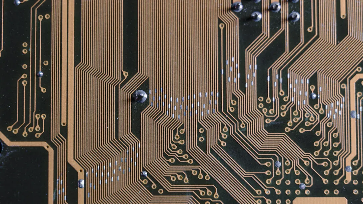
Trace width and spacing considerations
The size and space of traces are very important. They help control impedance in PCB production. You must calculate these carefully to meet the target impedance. For example, a 50-ohm impedance needs spacing 1x to 2x the trace width. Higher values, like 90-100 ohms, may need spacing up to 4x the trace width.
Designers use tools like field solvers or calculators to plan trace sizes. These tools show how width, height, and spacing affect impedance. If the measured impedance is correct, the PCB passes quality checks. If not, changes or fixes are needed.
Target Impedance | Spacing |
|---|---|
50 Ohms | 1x-2x trace width |
75 Ohms | 2x-3x trace width |
90-100 Ohms | 3x-4x trace width |
For fast PCBs, trace size also affects signal quality. Bad spacing can cause crosstalk, which makes signals unclear. By following the right trace rules, you keep impedance steady and improve performance.
Dielectric thickness and material properties
The insulating material in a PCB affects impedance control a lot. Its thickness and dielectric constant (Dk) decide how signals move through the board. Materials with low, stable Dk are easier to use and give better results.
Thicker insulating layers can improve impedance. For example, thicker materials lower the difference between the electrode and surface. This shows why choosing the right material and thickness is so important.
The prepreg material’s dielectric constant changes impedance values. Picking stable materials helps control the final product better.
For fast PCB designs, pick materials that reduce signal loss. This helps meet the strict needs of modern electronics.
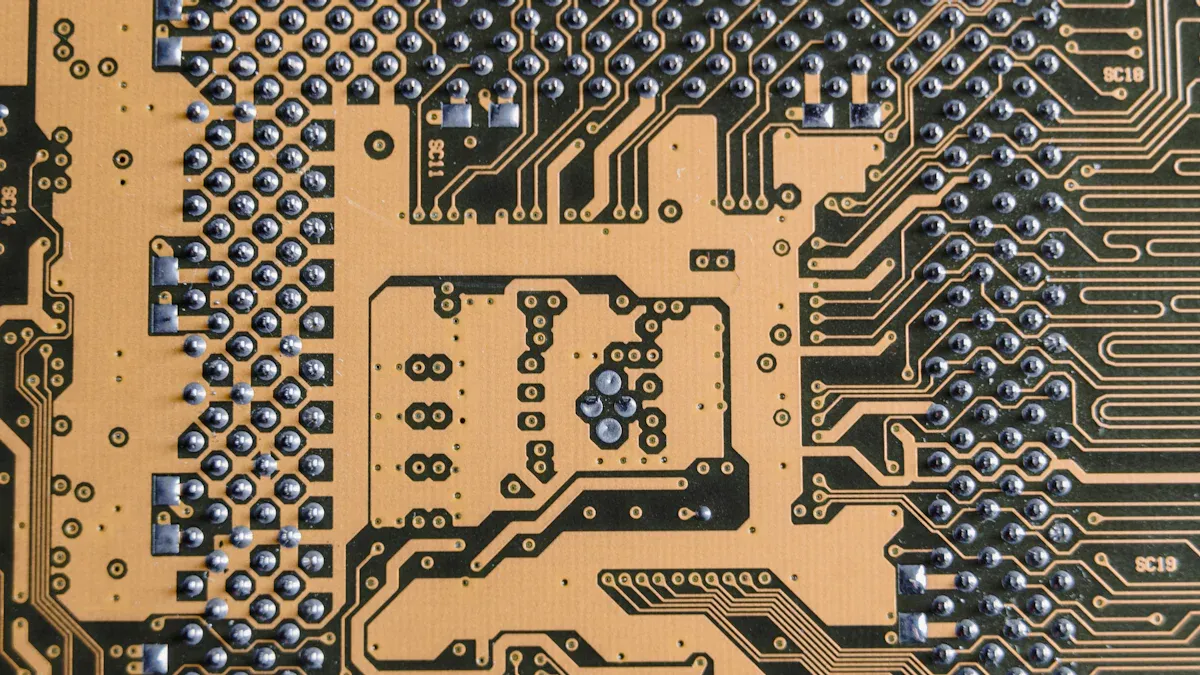
Routing layer and stack-up planning
Planning the routing and stack-up is key for multi-impedance control. You must organize the PCB layers to match the needed impedance. This means picking materials that fit the transmission line’s loss budget and PCB type, like HDI.
Tools like IPC-2141 formulas, stack-up planners, or field solvers can help. They let you test the routing and see how the stack-up affects impedance.
Pick materials that keep the transmission line within the loss budget.
Use an accurate impedance calculator for early designs.
Test the routing to confirm the design works.
Good stack-up planning also balances layers to stop warping and improve signals. By focusing on routing and stack-up, you can make PCBs for high-speed uses.
Designing for controlled impedance requirements

Why stack-up planning matters for multi-impedance control
Stack-up planning is key to meeting impedance needs in PCBs. It arranges PCB layers to match high-speed application goals. Without good planning, signals can get distorted, causing performance problems.
To design a good stack-up, decide the layer structure early. This means choosing dielectric thickness, materials, and routing layers. Sharing these details clearly avoids production delays.
For example, unclear impedance details can cause big problems. A front-end engineer might face delays figuring out which layers need impedance control and the right trace widths.
You can avoid such problems by giving clear details like:
Trace width and spacing.
Layers needing impedance control.
Material properties like thickness and dielectric constant.
By focusing on these points, your PCB will meet impedance needs and work well in fast systems.
Picking materials for steady impedance
Choosing the right materials keeps impedance steady across your PCB. Dielectric thickness and material type affect signal quality and impedance control.
Factor | What It Affects |
|---|---|
Dielectric Thickness | Changes transmission line impedance, especially in high-frequency circuits. |
Material Composition | Resin, glass, or filler types affect how thickness is controlled during production. |
For fast systems, pick materials that reduce impedance changes. These changes can cause signal issues and slower data speeds. To keep impedance steady, follow these steps:
Check your system’s frequency range and loss limits.
Set key needs like insertion and return loss.
Think about costs and environment when picking materials.
By doing this, your PCB will meet impedance needs and work well in fast systems.
Using tools to check impedance
Simulation tools help check and model impedance in PCB designs. They show how your design will work in real life. This ensures it meets impedance needs.
Tool accuracy depends on factors like material models and adjustments. For fast designs, broadband dielectrics and roughness models are important. These models handle material and shape changes, giving accurate results for speeds up to 448 Gbps.
Broadband material models use GMS-parameters for automatic setup. They separate losses from materials and conductors, making reliable models for fast systems.
With simulation tools, you can check impedance goals and spot problems early. This saves money and ensures your PCB works well in fast digital systems.
Documentation needs for multi-impedance control
Fabrication notes and details
Clear notes are key for good impedance control in PCBs. These notes help manufacturers follow your design needs. Include details like material type, copper weight, and layer count. List important factors such as target impedance, trace width, height, and Z-axis distance. If using differential or coplanar traces, add copper-to-copper spacing info.
Also, mention any special material needs, like low dielectric constant (Dk) or dissipation factor (Df). This ensures materials match your impedance goals. Giving these details reduces mistakes during production and keeps signals clear in your PCB.
Impedance tables and limits
Impedance tables are helpful for designers and manufacturers. They show the impedance needs for each PCB layer. A good table should include:
Specification Element | Description |
|---|---|
Impedance Value | The target impedance for the traces. |
Trace Width | The trace width needed for the impedance. |
Differential Pair Spacing | The space between pairs for controlled impedance. |
Layer | The layer with controlled impedance traces. |
Standard Tolerance | ±10% ohms, or ±5% ohms for stricter needs. |
Following these specs ensures the process matches your design. This focus keeps signals strong and makes sure the PCB works well.
Work statements for manufacturers
A clear statement of work (SOW) is very important. It explains all impedance control needs to the manufacturer. Include materials, stack-up plans, and testing methods. Add any special steps needed to meet impedance goals.
A detailed SOW avoids confusion and helps manufacturers understand your needs. This document acts as an agreement, ensuring both sides deliver a quality PCB that meets all requirements.
Common challenges in achieving multi-impedance control
Changes in manufacturing processes
Manufacturing changes can affect impedance control in PCBs. Copper thickness is a big factor. A 10% change in copper thickness can shift impedance by 2-3%. For fast designs, tight tolerances like ±5% are common. Small changes can mess up signals and cause problems.
Plan for these changes during the design stage. Work closely with your fabricator to meet copper thickness needs. Use stricter controls, like making impedance coupons, to check accuracy. But, larger coupons take up space, so plan carefully.
Poor communication between designers and fabricators
Bad communication between designers and fabricators causes impedance issues. If design limits don’t match what manufacturers can do, the PCB may fail. For example, unclear trace width or spacing details can delay production or cause mistakes.
To fix this, share clear notes and plans with your fabricator. Include fabrication notes, impedance tables, and stack-up details. This helps both sides understand the needs and keep signals strong. Teamwork is important for solving problems in complex PCB designs.
Environmental effects on impedance
The environment can also change impedance. Temperature and humidity can affect PCB materials. These changes can alter the dielectric constant and disrupt signals. Fast designs are especially sensitive to these changes.
To reduce these effects, pick materials with stable properties. You can also use air-gap methods to improve signal stability. These steps help your PCB work well, even in tough conditions.
Verification and testing methods for multi-impedance control
Test coupons for impedance validation
Test coupons help check impedance in PCB production. These small PCB sections copy the impedance setup of the real design. They are used to see if the transmission lines meet the needed standards. Manufacturers often use Time-Domain Reflectometry (TDR) to test these coupons. TDR measures the impedance of the PCB’s lines and keeps signals clear for fast circuits.
For high-frequency designs, testing impedance is even more important. TDR checks the test coupon’s special traces to confirm the PCB meets impedance rules. By testing these coupons, you can avoid signal problems and ensure the PCB works correctly.
Measurement tools and techniques
Good tools are needed to measure impedance accurately. The FFT-based system is very precise, with only 1.6% error for size and 0.751° for angle. Other methods, like Gain Phase Detector (GPD) and I-Q Demodulation, have bigger errors—5.1% and 8.1% for size.
The FFT-based method also uses less power, needing only 122.4 mW. GPD uses 159.2 mW, and I-Q needs 290.5 mW. But FFT-based tools need advanced processing to fix spectral leakage. Picking the right tools helps you measure impedance well and control your PCB design.
Ensuring compliance with design specifications
Meeting design rules is key for keeping impedance steady in PCBs. Impedance standard substrates help check and adjust circuit impedance. These tools reduce signal loss, reflections, and electromagnetic interference (EMI), keeping signals strong in fast designs.
Things like trace size, signal spacing, and material properties affect compliance. For example, keeping impedance steady across lines stops reflections and keeps signals clear. By following these rules, you can make PCBs that work well in modern electronics.
Understanding multi-impedance control in PCB making needs careful planning. Focus on important things like picking materials, layer setup, and checking signals. Sharing clear details and good notes helps your PCB work well. LT CIRCUIT makes great PCBs with steady impedance, keeping signals strong for modern uses.
FAQ
What is multi-impedance control in PCB production?
Multi-impedance control keeps signal paths steady in a PCB. It stops signals from getting messed up and helps fast circuits work better.
Why is stack-up planning important for multi-impedance control?
Stack-up planning arranges PCB layers to match impedance needs. It keeps signals clear by balancing materials, thickness, and routing paths.
How do simulation tools help in achieving impedance control?
Simulation tools show how impedance works in PCB designs. They find problems early and check if the design meets impedance rules.
See Also
Enhancing Signal Integrity Through Impedance Control in PCBs
Understanding The Manufacturing Process Of Rigid-Flex Circuit Boards
Challenges And Solutions In Multi-Layer Circuit Board Prototyping
Addressing Common PCB Design Issues For SMT Technology Needs
A Comprehensive Guide To Heavy Copper Multilayer PCB Production