The manufacturing process and prototyping difficulties of multi-layer circuit boards
Multi-layer circuit boards are very important in today’s electronics. They have many layers of conductive material stacked on top of each other. This helps make devices smaller and work better. These boards are used in things like phones, medical tools, and cars.
The market for multilayer PCBs is growing fast because of new ideas and more need in telecom and car industries. However, the production process of making them is hard. It requires exact layer placement and tricky calculations, which makes testing them a tough job.
Key Takeaways
Multi-layer circuit boards are important for today’s electronics. They help make devices smaller and work better.
Making these boards needs good design, the right materials, and perfect layer placement to work well.
Testing multi-layer boards can be tricky. Problems like layers not lining up or uneven materials need special tests to fix.
The Production Process of Multi-Layer Circuit Boards
Design and Material Selection
Making multi-layer boards starts with planning and picking materials. You decide how the copper and insulating layers will be arranged. This setup affects how signals move and how easy it is to make. More layers are needed for complex designs or fast signals.
When choosing materials, think about heat, strength, and cost. For example:
Dielectric constant helps signals stay clear in fast systems.
Thermal management handles heat to keep the board working well.
Environmental conditions guide choices to reduce harm to nature.
Matching your design to what the factory can do makes production smoother. This step is key for creating a good-quality board.
Layer Alignment and Lamination
Aligning and sticking layers together is very important. If layers don’t match up, the board won’t work. Factories use holes to line up the layers of copper and prepreg sheets.
Lamination uses heat, pressure, and vacuum to stick layers together. This removes air bubbles and hardens the resin in the prepreg. To avoid bending, layers should be balanced. Using materials from one supplier also helps.
This careful process makes the board strong and ready for the next steps.
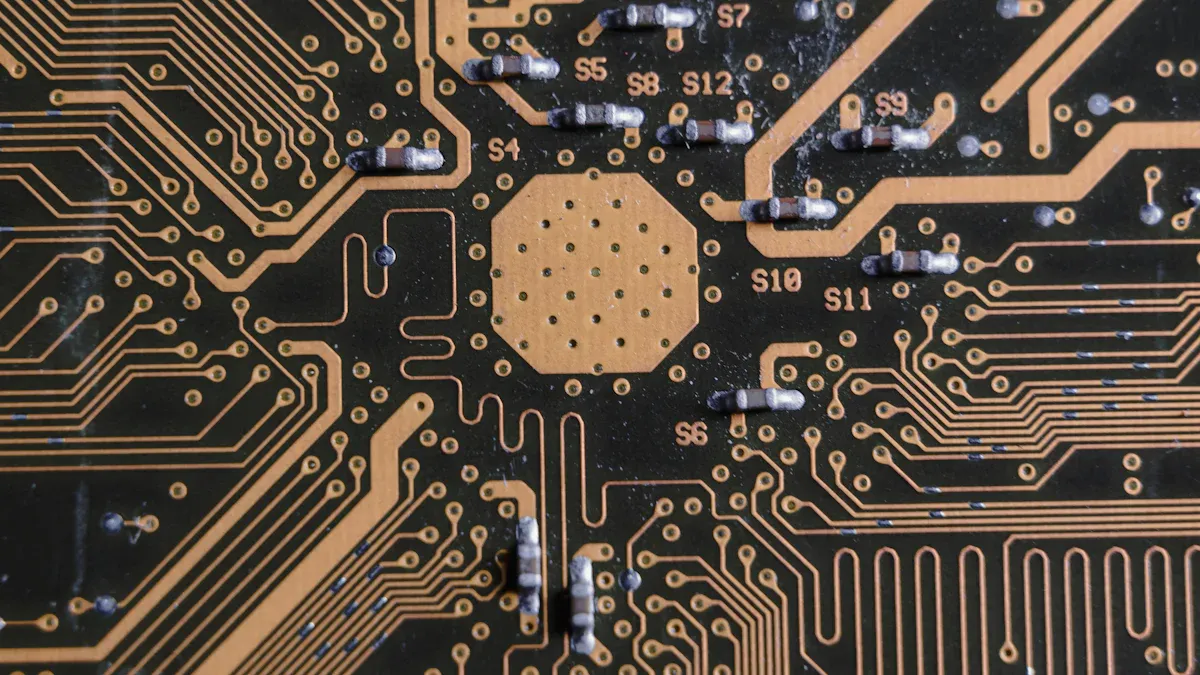
Etching and Circuit Formation
Etching creates paths for electricity to flow. It starts with a copper-covered material. A film is added and exposed to light or lasers to make patterns.
Afterward, extra copper is removed, leaving only the circuits. Sometimes, leftover copper can cause problems, so inspections are done.
This step needs accuracy because small mistakes can ruin the board. More layers mean more chances for errors, so checking quality is very important.
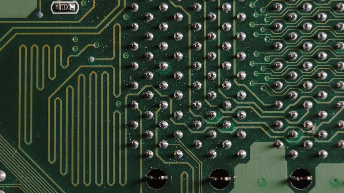
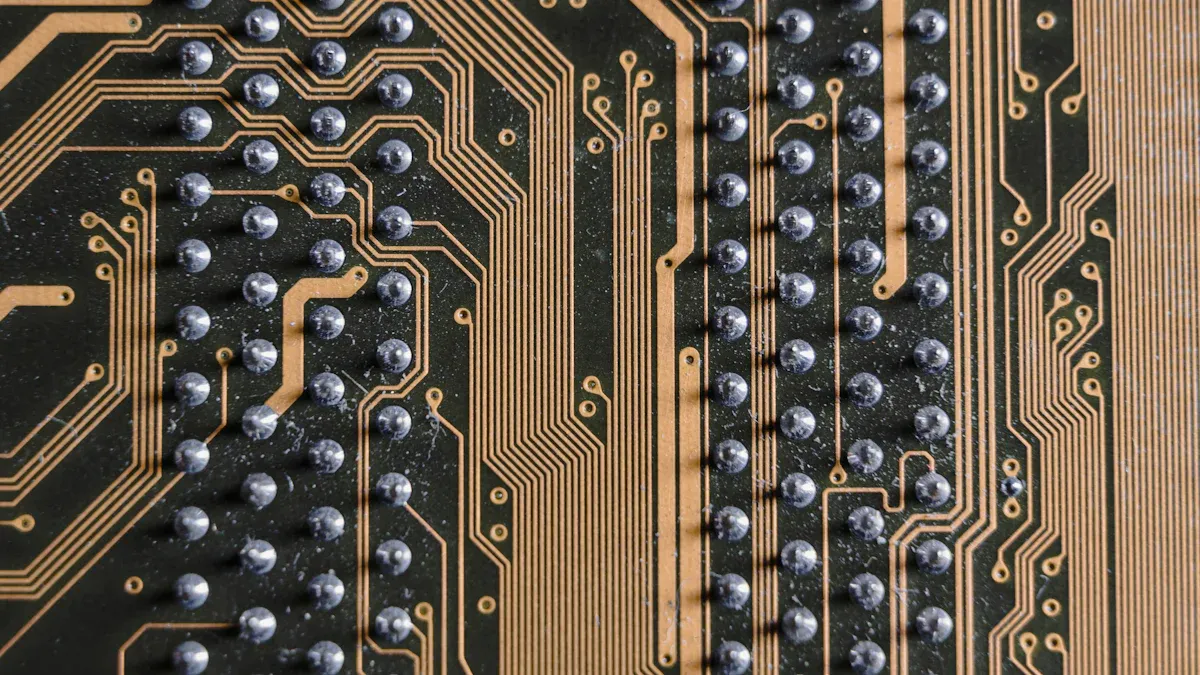
Drilling and Via Creation
Drilling makes connections between the board’s layers. Tiny holes, called microvias, are made with lasers for small designs. Plasma drilling helps create better shapes for more options.
Back drilling removes extra bits that can mess up signals. Machines drill many boards at once to save time.
Tools are checked during drilling to keep everything precise. These methods make sure the process is fast and correct.
Plating and Surface Finishing
Plating and finishing protect the copper parts of the board. These coatings stop rust and damage, making the board last longer. Popular finishes include ENEPIG and hard gold.
Surface Finish | Benefits | Downsides |
|---|---|---|
ENEPIG | Flat surface, no lead, great soldering | Costly, hard to fix |
Hard Gold | Strong, lasts long | Very pricey, takes time |
The finish you pick depends on cost, use, and environment. Good finishing improves how well the board works.
Quality Assurance and Testing
Testing makes sure the board meets all rules. Checks start before making the board to find problems early. During production, issues are fixed right away.
Important tests include:
Automated Optical Inspection (AOI): Finds mistakes like bad soldering.
Flying Probe Testing: Tests circuits on sample boards.
X-ray Inspection: Looks inside for hidden problems.
Test | What is Checked | Standard |
|---|---|---|
Finds dirt or damage | Pass/fail | |
Peel test | Checks layer strength | Pass/fail + value |
Electrical test | Tests all connections | Resistance <5Ω |
These tests make sure the board is safe and ready to use.
Prototyping Challenges in Multi-Layer Circuit Boards
Layer Misalignment Issues
Aligning layers in multi-layer boards is very important. Small misalignments can stop the board from working. This can happen during lamination or if materials are handled poorly. Misaligned layers may cause electrical paths to break, ruining prototypes.
To fix this, factories use special tools to align layers. But, as layers increase, misalignment risks grow. This makes production harder and needs more careful work.
Material Inconsistencies
Materials for multi-layer boards must meet strict rules. Bad materials can cause uneven thickness, poor heat control, or weak layer sticking. For example, if the dielectric constant changes, signals may not work well in fast circuits.
Finding special materials can also be tough. Rare materials may delay projects and cost more. Keeping material quality steady is key for good prototypes.
Testing and Debugging Limitations
Testing multi-layer boards is harder than single-layer ones. With many layers, finding and fixing problems is tricky. Defects inside layers are hard to spot. Simple tests like looking at the board don’t always work.
Advanced tools like X-ray inspection and flying probes are needed. These tools need experts and cost more money and time. Debugging multi-layer boards takes deep knowledge of their design.
Cost and Time Constraints
Making multi-layer boards costs a lot and takes time. Using thick copper layers can raise costs by 10-15%. If you need it faster, costs can go up by 10% to 50%. Complex designs also take longer to make.
Rushing orders for quick delivery can cost even more. Multi-layer boards need better designs and advanced methods. This makes prototyping take more time and money.
Tip: Plan your design well and work with skilled makers to handle these problems better.
LT CIRCUIT’s Skills in Making Multi-Layer PCBs
Modern Manufacturing Methods
LT CIRCUIT uses advanced ways to make multi-layer PCBs better. These methods save time and improve quality. For example:
HDI PCBs allow more wires, making designs smaller and lighter.
Micro via technology improves how signals move through the board.
Laser drilling cuts production time by nearly 40%, speeding things up.
Automated Optical Inspection (AOI) finds mistakes, reducing defects to under 1%.
These methods make electronics simpler and PCBs stronger. By using expert OEM services, LT CIRCUIT has made production 35% faster.
Smart Solutions for Prototyping Problems
Making multi-layer PCB prototypes is tricky, but LT CIRCUIT has smart fixes. They use special tools to align layers perfectly, avoiding errors. High-quality materials are chosen to stay consistent and meet strict rules.
To solve testing issues, LT CIRCUIT uses X-ray tools and flying probes. These tools find hidden problems and ensure prototypes work well. By improving the process, LT CIRCUIT saves time and money while giving reliable results.
Focus on Quality and Accuracy
LT CIRCUIT cares about quality and accuracy in every step. They follow strict rules to keep high standards:
Benchmark Type | What It Does |
|---|---|
Precise tools for etching and drilling keep circuits accurate and high-quality. | |
Strict Quality Checks | Tests are done at every step, like visual checks and reliability tests. |
Better Production Processes | Using smart systems and parallel work speeds up production and avoids delays. |
LT CIRCUIT also has certifications like ISO9001-2000 and UL Certification. These show they meet global quality rules. This ensures every PCB works well and meets your needs.
Making multi-layer PCBs needs careful steps, from planning to testing. Each step ensures the board works well. Prototyping has problems like uneven materials and hard-to-find errors. Success comes from accuracy, new ideas, and teamwork. LT CIRCUIT uses smart tools, skilled workers, and promises high-quality multi-layer PCBs.
FAQ
Why are multi-layer PCBs better than single-layer ones?
Multi-layer PCBs save room and work faster. They allow more connections and quicker signals. This makes them great for devices like phones and medical tools.
How is the quality of multi-layer PCBs checked?
Factories use special tools like X-rays and AOI machines. These tools find problems early to make sure boards are reliable and high-quality.
Why do multi-layer PCBs cost more?
Making them needs careful alignment, special materials, and tough tests. These steps make them pricier than single-layer PCBs.
See Also
Understanding The Manufacturing Steps For Rigid-Flex PCBs
Essential Skills For Designing Multi-Layer PCB Layouts
Exploring Multilayer PCBs And Their Role In Electronics