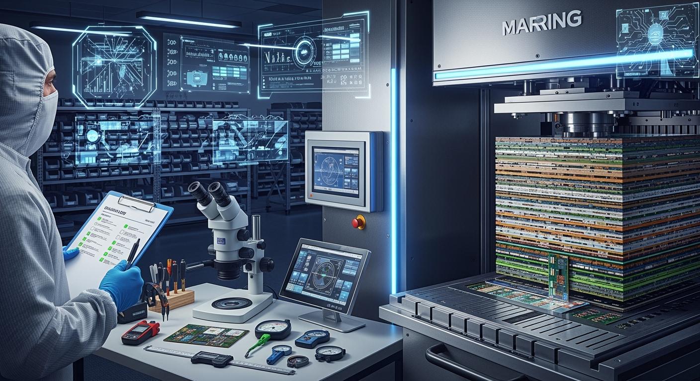
How to Optimize Multi-layer PCB Pressing for Quality
You can make the multi-layer pcb pressing process better by watching important settings. Temperature, pressure, time, and alignment change how many good printed circuit boards you get. They also change how good the boards are. Multi-zone vacuum lamination presses help you keep temperature and pressure steady. This helps the curing stay the same each time. Hydraulic presses and prepreg resin are important for sticking layers together. Careful control stops problems like delamination and warpage. Watching the glass transition temperature keeps the pcb strong. Look at the usual values below:
Parameter | Recommended Value |
|---|---|
Temperature | 180-200°C |
Pressure | 300-500 psi |
Time | 60-120 minutes |
Key Takeaways
Watch the temperature and pressure during pressing. The best settings are 180-200°C and 300-500 psi. These settings make boards strong and reliable.
Pick the right materials for your multi-layer PCB. FR-4 costs less and is strong. Polyimide works best when there is high heat.
Clean each layer well before lamination. Clean copper layers help resin stick better. This stops layers from coming apart.
Use optical registration and steel caul plates for good layer alignment. This stops layers from moving. It also makes copper plating better.
Write down details for every pressing cycle. Good records help find problems. They also help make production better next time.
Multi-layer PCB Material Preparation
Material Selection and Handling
You must pick the right materials for your multi-layer pcb. This helps make boards strong and reliable. FR-4 is the most common base material. It gives good strength and insulation. It also costs less than other materials. If you need special features, use polyimide for high heat. PTFE is good for low signal loss. Metal core boards help with heat in power electronics. Look at the table below to see important properties:
Material Type | Key Properties | Best Use Case | Cost Comparison |
|---|---|---|---|
FR-4 | Strong, good insulation, moderate heat | General electronics | Economical |
Polyimide | High heat, flexible, chemical resistant | Aerospace, medical | Higher than FR-4 |
PTFE | Low signal loss, low dielectric constant | RF, microwave | Most expensive |
Metal Core | Good heat dissipation, strong | LED, power supply | Varies |
Store pcb materials in a dry place. Keep the temperature steady. Humidity should stay between 40% and 65%. Use covers to keep dust away. Do not let sunlight touch the materials. Put unused boards in anti-static bags. Use racks that do not cause static. Label each board and check them often.
Layer Cleaning and Pre-treatment
Clean every copper layer before layup and lamination. Clean layers help resin stick better. This stops problems like delamination. You can use ultrasonic cleaning, vapor degreasing, or liquid immersion. These methods remove oils and dust from copper. If you skip cleaning, resin may not stick well. You could get corrosion or weak dielectric strength. Make sure copper is shiny and has no fingerprints before pressing.
Stack-up and Alignment Methods
Stack-up and alignment are important for dense circuits and strong boards. Place each printed circuit board layer in the correct order. Use steel caul plates to spread pressure evenly. This keeps the stack flat. Pin lamination works for most jobs. Optical registration gives the best accuracy, down to ±15 microns. Pinning and caul plates stop layers from shifting during pressing. Good alignment keeps copper plating and solder mask in the right place. This helps make high-quality pcb boards.
Key Parameters in Multilayer PCB Pressing
Temperature and Pressure Settings
You need to watch temperature and pressure to make strong multilayer pcb boards. For standard FR-4, the lamination temperature should be between 180°C and 190°C. High-Tg FR-4 needs a higher temperature, close to 200°C. The hot plate in the press stays between 180°C and 200°C. This temperature helps the prepreg resin move and harden the right way. Hydraulic presses or vacuum presses help keep the pressure even. Most presses use pressure from 300 psi to 500 psi. This pressure lets the resin fill spaces and stick copper layers together.
The best lamination temperature for standard FR-4 is 180°C to 190°C.
High-Tg FR-4 needs about 200°C for lamination.
The hot plate temperature is usually 180°C to 200°C (356°F to 392°F) for good resin flow and curing.
If you do not set these values right, you can get problems. Check the table to see what can go wrong if you miss the right settings:
Defect | Cause | Prevention |
|---|---|---|
Delamination | Incomplete cure, trapped moisture, poor prepreg | Pre-bake materials, control dwell time |
Resin voids | Trapped air, not enough pressure | Use vacuum lamination, adjust ramp-up |
Warpage | Uneven stack-up, uneven cooling | Make stack even, control cooling rate |
Inner-layer shift | Bad registration or too much pressure | Use optical registration, balanced lay-up |
Keep the temperature and pressure steady. This helps the resin harden and keeps copper layers from moving. You will have fewer problems and stronger printed circuit board stacks.
Pressing Time Control
You need to watch the pressing time during the process. The lamination cycle for multi-layer pcb boards takes about 4 to 6 hours. The design, number of layers, and special features like blind or buried vias can change the time needed. More layers or special parts may need extra cycles. Set the right dwell time so the prepreg resin gets hard all the way. If you go too fast, you can get delamination or weak copper bonds. If you wait too long, you can get warping or cracks in the resin.
Use a timer on the press to check each cycle. Watch the resin flow and make sure the copper layers stay flat. Vacuum pressing can help remove air and spread the resin. This step helps you make strong multilayers with good copper plating and solder mask.
Layer Alignment Accuracy
You need to keep each layer in the right spot during pressing. If you miss the alignment, you can get inner-layer shift or bad copper plating. New post-etch punch machines use cameras to check and fix layer problems. These machines look at each layer before lamination. If a layer is not right, you can take it out. Laser Direct Imaging (LDI) and Automated Optical Inspection (AOI) tools can find tiny mistakes, as small as 2 microns. Fixing problems early helps you waste less and get better solder mask and copper.
Use optical registration to line up the copper layers. Steel caul plates keep the stack flat. Pinning holds the layers in place. Check the alignment before and after pressing. This step helps you make high-quality multi-layer pcb boards with strong copper bonds and good solder mask.
Tip: Always check the alignment and pressing time for every batch. You can use cameras and AOI tools to find mistakes early. This step helps you stop problems and keeps your multilayer pcb boards strong.
Multi-layer PCB Pressing Process Steps
Loading and Pre-heating
You start the multi-layer pcb pressing process by preparing the layup. Place the core, prepreg, and copper foils in the correct order. Align each layer carefully to avoid shifting during pressing. Use steel caul plates and pins to keep everything in place. Once you finish the stack, load it into the lamination press. Pre-heating begins as soon as you close the press. The heat softens the prepreg resin and helps it flow between the copper layers. This step removes moisture and air, which can cause defects in the final board production.
Tip: Always check the temperature before starting. Pre-heating at the right level helps the resin flow and stick to the copper.
Pressing Cycle Execution
You now start the main pressing cycle. The press applies heat and pressure to the stack. Vacuum pressing works best for multilayer pcb boards. It removes air and volatiles from between the layers. This step reduces the defect rate and helps the resin fill every gap. You get a uniform dielectric layer, which improves high-frequency signal performance. The press keeps the pressure steady, usually within ±5%. The resin cures and bonds the copper layers together. This creates a strong mechanical and electrical connection.
Here are the main steps in order:
Align the stackup with copper, prepreg, and core.
Load the stack into the press.
Apply heat and pressure.
Use vacuum to remove air and help resin flow.
Cure the resin to bond the layers.
Cooling and Unloading
After the resin cures, you must cool the printed circuit board slowly. Controlled cooling prevents warping and keeps the board flat. The ideal cooling rate is 1–3°C per minute. This rate stops internal stress and avoids cracks or delamination. Keep the pressure on during cooling to maintain the shape. When the board reaches room temperature, you can unload it from the press.
Aspect | Details |
|---|---|
Ideal Cooling Rate | 1–3°C/min |
Benefits | Prevents internal stress and warpage |
Result | Ensures dimensional stability and flatness |
You now have a stable multilayer pcb panel ready for solder mask and final board production. Careful control at each step gives you strong copper bonds and reliable multilayers.
Quality Control and Troubleshooting
In-process Monitoring
You have to watch the process closely to keep multilayer pcb boards good. People check every step, like pattern imaging, lamination, and making the final board. Process control helps keep settings the same and makes boards more alike. Online inspection uses X-ray and special cameras to find problems early. Watching all the time helps you catch mistakes before they hurt the printed circuit board. Some common tests are In-Circuit Testing, Functional Testing, Flying Probe Testing, and automated optical inspection. For high-speed boards, signal integrity testing checks for crosstalk and impedance. You need to keep these numbers within plus or minus 10% of 50 ohms.
Technique | Description |
|---|---|
Production Line Monitoring | Watches all steps, like sampling, printing, etching, drilling, assembly, and soldering. |
Process Control | Keeps production steady and makes products more alike. |
Online Inspection | Uses X-ray and cameras to find problems fast. |
Tip: Watching the process all the time helps you find problems early and keeps multilayer boards strong.
Post-press Inspection
After lamination, you must check the pcb for problems. X-ray imaging looks for empty spots inside and layers that do not line up. Acoustic microscopy finds delamination without hurting the board. Automated optical inspection looks for surface problems and layers that are not lined up. Ultrasonic testing uses sound waves to find empty spots or delamination inside. You have to check copper bonds, solder mask, and if layers are lined up. The last check uses industry rules to see if the board is good.
Class | Description | Acceptance Criteria |
|---|---|---|
Class 1 | Works okay; looks do not matter if it works. | Small flaws are okay. |
Class 2 | Must keep working; some flaws are okay. | Rules are stricter than Class 1. |
Class 3 | Must work all the time; no breaks allowed. | Has to work well in every case. |
Note: Always write down inspection results and keep records for each pcb.
Common Defects and Solutions
You might see problems like delamination, voids, warping, or registration issues in multi-layer pcb pressing. Delamination happens from water, bad sticking, or heat stress. Voids show up when air gets trapped or resin does not move right. Warping comes from uneven materials or cooling the wrong way. Registration issues happen when machines are not lined up or copper shrinks.
Defect Type | Root Causes |
|---|---|
Delamination | Water, bad sticking, heat stress |
Voids | Trapped air, not enough resin, bad materials |
Warpage | Uneven materials, wrong cooling, materials do not match |
Registration Issues | Machines not lined up, copper shrinks, people make mistakes |
You can stop resin starvation by changing resin amount, fixing pressure, and adding dummy copper. To fix warping, balance copper, use even stack-up, and cool down slowly. Always track each step with barcodes or RFID for records. Write down what you do, machine settings, and quality checks. Industry rules like IPC-2221, ISO 9001, and UL Certification help you keep boards good.
Tip: Good records and tracking help you fix problems faster and make better boards next time.
You can get good printed circuit boards by paying attention to each step. The table below shows important ways to help:
Key Aspect | Description |
|---|---|
Stack-up Symmetry | Balanced layers stop warping and help signals return. |
Material Selection | Using similar materials keeps boards from warping. |
Design for Manufacturability | Following DFM rules makes boards easier to build and more reliable. |
Keep your pcb dry and cool. Always check and test your boards carefully. If you keep improving, you will make fewer mistakes. You will finish boards faster and get better quality as time goes on.
FAQ
What is the main cause of delamination in multi-layer PCBs?
Delamination happens when water stays in the layers. It can also happen if the pressing temperature is wrong. Dry your materials before you start. Always check your press settings to help stop this problem.
How do you ensure proper layer alignment during pressing?
You can use steel caul plates or pins. Optical registration systems also help. These tools keep each layer in the right spot. Good alignment makes your board better.
Why is vacuum pressing important for multi-layer PCBs?
Vacuum pressing takes out air and water. This helps the resin move and fill all spaces. You get fewer empty spots and stronger boards.
What should you check after pressing a multi-layer PCB?
Look for delamination, empty spots, warping, and layers not lined up. Use X-ray or optical tools to check. Good checks help you find problems early.
Can you reuse leftover prepreg or copper foil?
Do not reuse leftover prepreg or copper foil. Old materials can take in water or lose quality. Always use new materials for the best boards.
See Also
Excelling in PCB Production Using Press-Fit Hole Techniques
Achieving Excellence in PCB Manufacturing Through Quality Control
Comprehensive Guide to Heavy Copper Multilayer PCB Production
Understanding the Manufacturing Process of Rigid-Flex Circuit Boards
Essential Skills for Designing Multilayer PCB Layouts Effectively