How multi-layer PCB solves the problem of withstand voltage between layers
Multi-layer pcb technology helps engineers fix voltage problems in printed circuit boards. New materials and careful steps make things safer. Good insulation keeps each printed circuit board layer apart. LT CIRCUIT gives strong multi-layer pcb solutions. Printed circuit board uses need careful planning for each pcb. Printed circuit boards need accuracy to last long.
Key Takeaways
Using good dielectric materials and the right insulation thickness keeps each PCB layer safe from high voltage and stops electrical breakdown.
Careful design of the space between layers and the order of stacking lowers noise, prevents shorts, and makes the PCB stronger and work better.
Careful testing and strong quality checks find weak spots early, so multilayer PCBs last longer and work well even in hard situations.
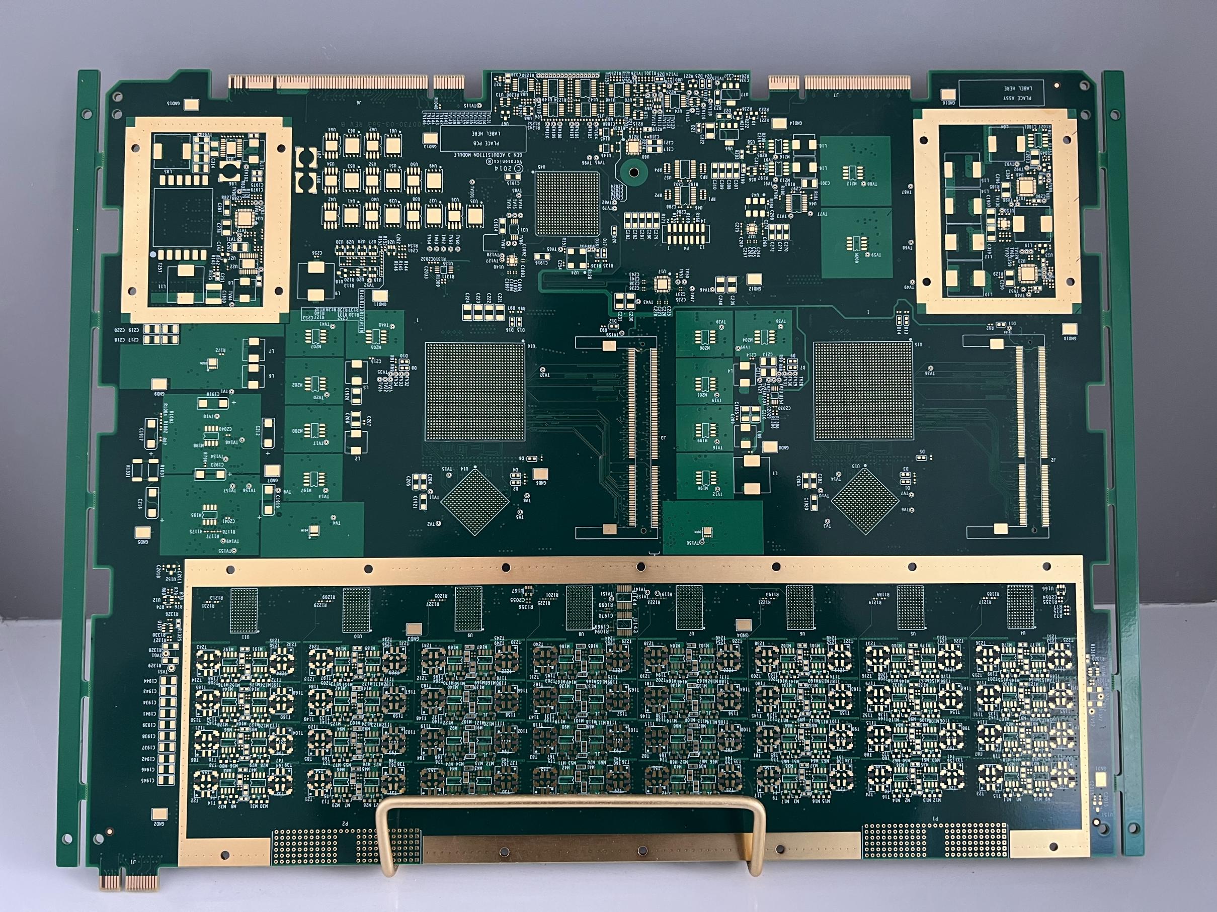
Multilayer PCB Structure
The way a multilayer PCB is built helps stop voltage problems between layers. Engineers make these printed circuit boards with layers of copper and insulation. Each layer stays apart and safe, even with high voltage.
Dielectric Materials
Dielectric materials are very important for insulation in multilayer PCBs. Makers often use epoxy resin with fiberglass, called FR-4, for these layers. This material keeps copper layers apart and stops unwanted electricity flow. New studies show that adding special nanoparticles can make dielectric materials work better. These new materials help printed circuit boards handle more voltage. LT CIRCUIT uses top-quality dielectric materials in every multilayer PCB. This choice makes the boards work well and last longer.
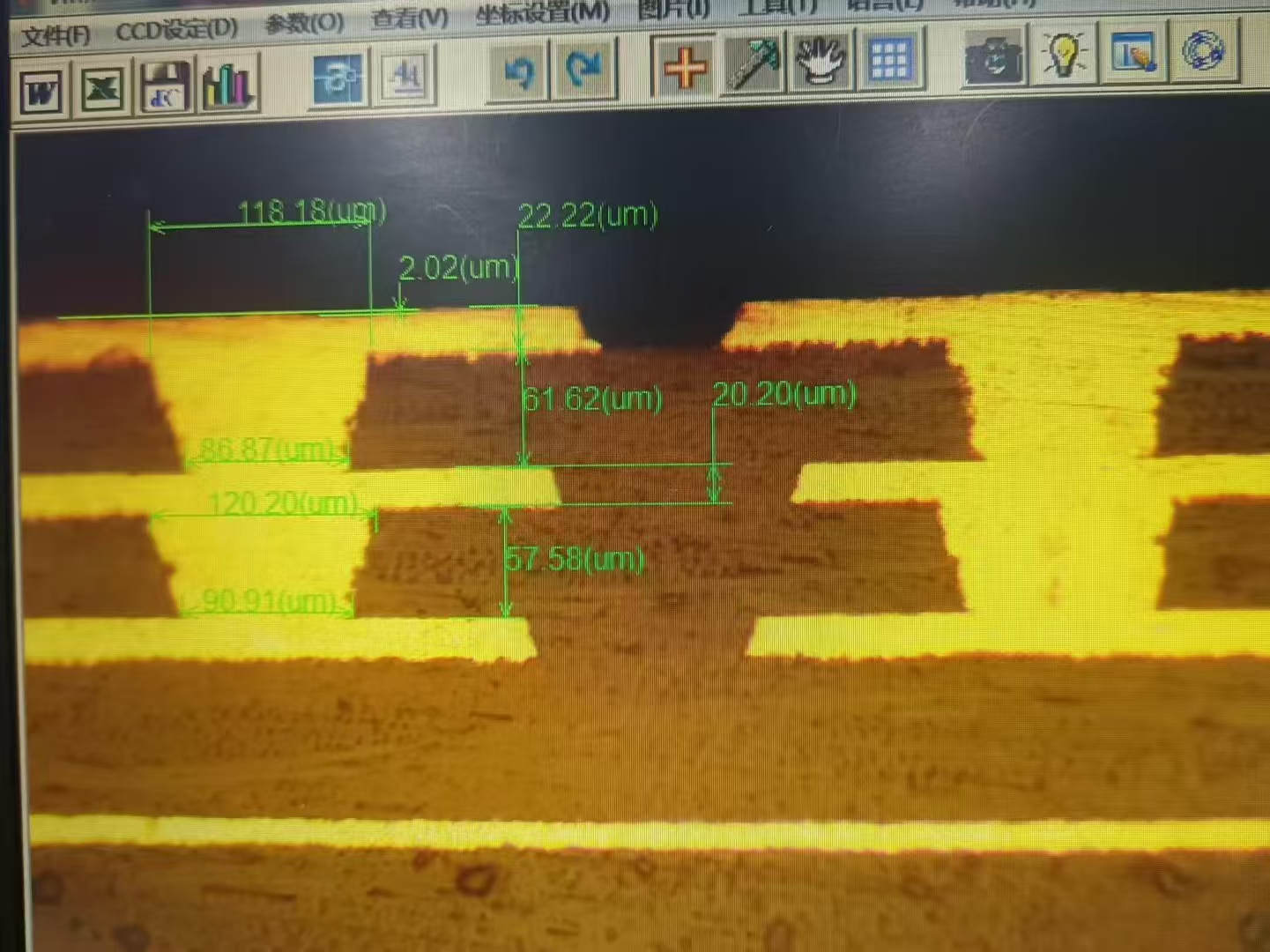
Insulation Thickness
Insulation thickness matters a lot in multilayer PCB design. Thicker insulation gives better protection from electrical problems. Engineers pick the right thickness for the voltage the board will face. If insulation is too thin, electricity might jump between layers and break the board. LT CIRCUIT checks each insulation layer carefully during making. This careful work helps the board handle high voltage and stay safe.
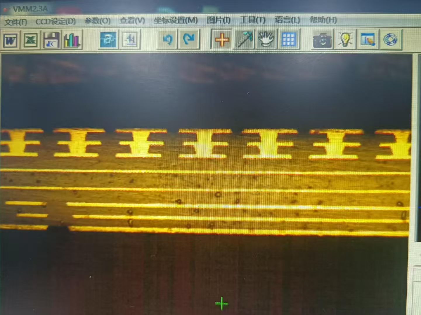
Layer Spacing
Layer spacing means how far apart the copper layers are in a multilayer PCB. Good spacing stops arcing and short circuits, especially with high voltage or high frequency. Industry rules, like IPC-2221, help engineers pick the right spacing for each board. Things like voltage, humidity, and material type change how much space is needed. LT CIRCUIT follows these rules and uses special tools to line up and press the layers. This careful work gives strong insulation and good electrical connections.
Tip: Always use the right rules for layer spacing and insulation thickness. This helps multilayer PCBs work better and stay safe.
A multilayer PCB’s structure, with good dielectric materials, the right insulation thickness, and careful layer spacing, helps the board handle high voltage. LT CIRCUIT’s use of new materials and careful building makes sure each multilayer PCB has strong insulation, good heat flow, and works well for tough jobs.
Design and Manufacturing for High-Quality Insulation
Stack-Up Design
A good stack-up design helps make strong insulation. Engineers put copper and dielectric layers in a special order. They put signal layers next to power or ground layers. This keeps signals clear and lowers noise. Making the stack-up even stops bending and keeps the board flat. LT CIRCUIT uses smart design rules to meet tough standards.
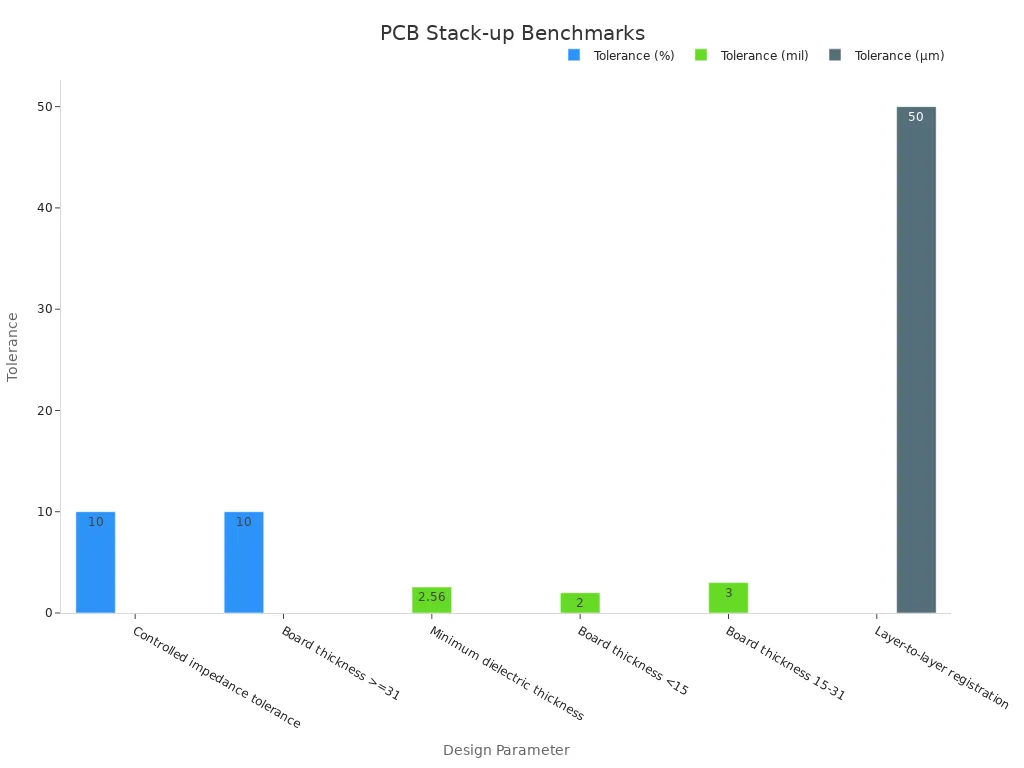
Benchmark / Tolerance | |
|---|---|
Controlled impedance tolerance | ±10% |
Minimum dielectric thickness | 2.56 mil (for IPC class 3 boards) |
Layer-to-layer registration | Up to 50µm (1.9685 mil) |
Board thickness tolerance (<15 mil) | ±2 mil |
Board thickness tolerance (15-31 mil) | ±3 mil |
Board thickness tolerance (≥31 mil) | ±10% |
Engineers do not put two signal layers together. This stops crosstalk and keeps connections strong. They use solid ground planes under important traces. This keeps impedance steady and makes the board work better.
Clearance and Separation
Clearance and separation rules keep insulation safe in multilayer pcbs. The smallest drill-to-copper clearance is 8 mil. This space helps with small moves during drilling and pressing. LT CIRCUIT follows IPC-2221 and IPC-2222 rules for these spaces. They use the "anti pad" method to keep copper away from via barrels. This stops shorts and keeps the board safe.
Standard | Scope | Key Considerations |
|---|---|---|
IPC-2221 | General PCB design requirements | Tolerances for hole sizes, trace widths, and layers to ensure manufacturability and performance |
IPC-2222 | Multi-layer PCB design requirements | Layer alignment, via placement, and drill tolerances critical for multilayer PCB integrity |
UL Certification | Safety and performance validation | Ensures material flame resistance and electrical performance, influencing achievable tolerances |
Engineers check finished hole size and plating thickness too. They often use a bigger clearance, like 9 mil, for safety and good performance.
Tip: Always follow the right rules for clearance and separation. This helps stop electrical problems and keeps insulation strong.
Lamination Process
The lamination process sticks all the layers together. LT CIRCUIT uses high heat and pressure to press the layers. They control the heat, usually from 170°C to 180°C. Pressure is between 200 and 400 PSI. Vacuum removes air bubbles that can make weak spots. Cooling is controlled to stop cracks or layers coming apart.
Description | |
|---|---|
Dielectric Constant (Er) | Stability of dielectric constant affects impedance and signal integrity; minimal fluctuations desired. |
Surface Resistivity | Electrical insulation resistance; ideal range 10^3 to 10^9 megaohms/m²; affected by moisture and heat. |
Flammability | Resistance to ignition; material should not burn more than 10 seconds after flame removal. |
Moisture Absorption | Ability to resist moisture; typical values 0.01% to 0.2%, lower is better. |
Chemical Resistance | Resistance to chemical absorption; should not exceed 0.2%. |
Time to Delaminate | Duration material withstands thermal shock or moisture before delaminating. |
Glass Transition Temperature (TG) | Temperature above which substrate softens; critical for manufacturing process selection. |
Coefficient of Thermal Expansion (CTE) | Degree of expansion under heat; important for microelectronics PCBs. |
Thermal Conductivity (k) | Heat transfer capability; low values indicate stable heat transfer under temperature rise. |
Copper Foil Peeling Strength | Bond strength between copper foil and base material; affected by foil thickness. |
LT CIRCUIT uses oxide treatment to make the bond stronger. This stops layers from coming apart and keeps insulation tight. They use special tests to find weak spots or empty spaces. These tests help make sure every board has good insulation and strong connections.
Testing and Quality Control
Testing and quality control are very important for multilayer pcbs. LT CIRCUIT uses many tests to check insulation and how the board works. Microsectioning cuts the board to show the inside. This test checks if layers line up and if there are empty spaces or layers coming apart. Electrical tests, like flying probe and E-test, check for good connections and find problems.
Thermal stress testing heats and cools the board many times. This checks if insulation stays strong when it gets hot or cold. Special tests, like X-ray CT and ultrasonic testing, find hidden problems inside the board. The Surface Insulation Resistance (SIR) test checks if insulation stops electricity from leaking.
LT CIRCUIT also uses the Wetting Balance test to check soldering. This test makes sure the board can be soldered without hurting the insulation. All these steps help LT CIRCUIT make multilayer pcbs that are strong, work well, and last a long time.
Note: Careful testing and strict quality control help stop problems like layers coming apart and electrical breakdown in multilayer pcbs.
Multilayer PCB Challenges and Tips
Common Issues
Multilayer PCB designs can have many problems. These problems can hurt insulation and make the board less reliable. Engineers often see things like dielectric breakdown and delamination. Thermal stress is also a big problem. If parts are too close, the board can fail faster. Heat from one part can affect another part nearby. This is called thermal crosstalk. Over time, insulation resistance can get worse. Some common problems are:
Heat and temperature changes can break the board.
Shaking can damage pads, vias, and solder joints.
The board can break during use or when being put together.
Bad spacing and poor heat control can cause more failures.
Engineers use special tests to find these problems early. They use tests like accelerated life testing and thermal cycling.
Design Tips
Engineers can make multilayer PCBs work better and safer. They should:
Put more space between parts to stop heat problems.
Use thermal vias to move heat away from hot spots.
Pick materials that move heat well and do not expand much.
Plan insulation thickness and layer spacing for the right voltage.
Use thermal cameras and sensors to find hot spots.
Tip: Good heat control and careful spacing help stop many failures in multilayer PCBs.
LT CIRCUIT Solutions
LT CIRCUIT uses smart design and building steps to fix these problems. Their team picks strong materials and plans the stack-up for each board. They use special computer tools to see how heat moves in the board. This helps stop overheating. LT CIRCUIT gives custom solutions for tough jobs. They use special insulation and extra tests when needed. Their strict checks make sure every board is safe and works well. Customers get boards that last longer and work better.
Engineers make insulation strong by picking good dielectric materials. They also keep layers apart and follow important design rules.
LT CIRCUIT gives advanced multilayer PCB solutions. They use careful testing and check quality to make sure boards work well.
Remember: Using these smart steps helps every designer build PCBs that are safer and last longer.
FAQ
What makes multilayer PCBs better at handling high voltage?
Engineers pick special dielectric materials. They also set the layers apart just right. These things help stop electrical breakdown. Each layer stays safe from high voltage.
How does LT CIRCUIT test insulation quality in multilayer PCBs?
LT CIRCUIT uses flying probe tests and E-tests. They also use microsectioning to look inside the board. These tests check if the insulation is strong. They help find weak spots that could cause problems.
Why is insulation thickness important in multilayer PCB design?
Thicker insulation keeps the board safer. It stops electricity from moving between layers. This helps the board last longer and work well.