Multi-material PCB Stack-up Design Techniques
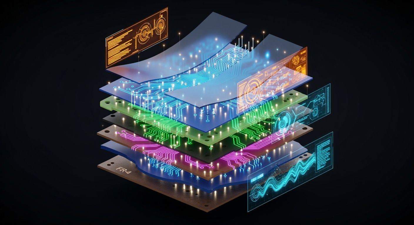
Multi-material pcb stack-up design combines different base layers like standard FR-4, Rogers PTFE, and flexible Polyimide into one printed circuit board. You build this strong pcb stack-up by carefully matching thermal expansion rates and choosing compatible bonding prepregs. You also balance dielectric constant and dissipation factor values across dielectric layers to protect high-speed signal integrity. This smart stack-up design improves high-frequency routing, speeds up heat loss, and strengthens overall board structure. You use advanced pcb layering to get top electrical performance without raising manufacturing costs. A balanced stack-up ensures long-term physical reliability and high production results for your modern high-density electronic devices.
Key Takeaways
Combine FR-4 with unique high-frequency materials to cut costs while maintaining fast signal speeds.
Keep the circuit board layout balanced from top to bottom so the board does not bend.
Clean smooth plastic surfaces with plasma before pressing layers together to build strong bonds.
Put solid ground layers directly beside signal lines to stop unwanted electrical noise.
Material Selection for Multi-Material PCB Stack-Up
Balancing High-Frequency Substrates and Standard FR-4
Combining costly high-frequency layers with standard FR-4 helps lower overall build expenses. Rogers RO4350B costs between $20 and $50 per square foot, whereas FR-4 is far cheaper. You save high-grade materials for main signal lines and use FR-4 for inner power planes. This clever stack-up setup keeps high-speed performance high while cutting total costs.
Before picking core materials, you should check how dielectric properties shift at different frequencies. The dielectric constant of FR-4 decreases as operating frequencies go higher.
Frequency | Dielectric Constant (Dk) | Dissipation Factor (Df) |
|---|---|---|
1 GHz | 4.35 | 0.022 |
5 GHz | 4.25 | 0.025 |
10 GHz | 4.20 | 0.028 |
20 GHz | 4.15 | 0.030 |
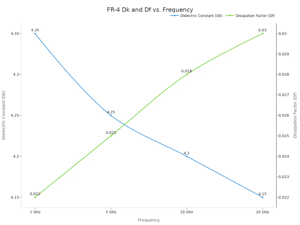
These property changes alter impedance control where different layers meet. Random shifts like these weaken signal quality in fast electronic devices.
Integrating Flexible and Rigid Materials
Polyimide film links directly with hard cores inside advanced circuit board designs. Flexible parts replace bulky wire connectors, while rigid areas hold heavy surface-mount items. Smart layer techniques hold these different materials together safely. You need matching prepreg adhesives to create a solid board structure. Pressed no-flow prepreg with coverlay achieves a typical peel strength of 6 Lb/in under IPC-TM-650 2.4.8 test standards.
Matching heat expansion rates stops inner layers from breaking during soldering heating cycles. Proper layering keeps thermal growth steady across the whole board. Unmatched expansion creates harsh physical stress that damages fragile connections. Careful material choices protect signal quality in sensitive high-speed circuits. Equal layout symmetry keeps the final board completely flat, preserving steady signal paths through every section. A smart layout ensures strong physical bonds and smooth electrical pathways, reducing factory defects to boost production success.
Symmetry and Layering Rules in Advanced PCB Layering
CTE Matching and Warp Prevention in Stack-Up Design
Making a multi-material circuit board needs putting together copper foil, prepreg dielectric materials, and core laminate sheets with bonded copper layers. You stack these dielectric sheets to form the basic physical frame. But heat brings mechanical tension since diverse materials stretch at different speeds. The Coefficient of Thermal Expansion (CTE) of copper measures ~17 ppm/°C. FR-4 measures 12 - 15 ppm/°C across the X/Y plane, but its Z-axis stretch hits 50 - 70 ppm/°C under its glass transition temperature. Over this glass transition range of 130-140°C, Z-axis stretch jumps to 250 - 300 ppm/°C.
According to IPC-6012, the maximum bow and twist shall be no more than 0.75% for surface mount assembly printed boards.
Unequal copper spacing through your pcb stack-up causes strong sideways stress during hot press steps. High reflow thermal stress near 260°C raises bending danger up to 20% in uneven boards. Tests on 100 mm x 100 mm boards show real thermal bending hits 0.5 mm in uneven builds, but falls to near 0.2 mm in balanced builds.
Substrate Property or Metric | Baseline Specification Value | Standard Thermal Impact |
|---|---|---|
Copper CTE | ~17 ppm/°C | Reference expansion baseline |
FR-4 Z-Axis CTE (Below Tg) | 50 - 70 ppm/°C | Normal thermal expansion range |
FR-4 Z-Axis CTE (Above Tg) | 250 - 300 ppm/°C | Extreme expansion above 130-140°C Tg |
IPC-6012 SMT Board Warpage Limit | 0.75% | Maximum permitted bow and twist |
IPC-6012 Non-SMT Board Limit | 1.5% | Standard assembly limit |
Symmetrical Architecture and Layer Balancing
Following proper pcb layering rules holds your board level during factory production and heat setup. You should match prepreg thicknesses, core laminates, and copper weights across the middle neutral plane of your stack-up. A smooth pcb stack-up structure built with an even number of layers cuts total board bending by 40–60%. Layouts using even layer counts keep overall bending under 0.7% because physical pulls stay balanced on both sides.
+-------------------------------------------------------+  Layer 1: Top Signal Layer (1 oz Cu)
=========================================================  Prepreg Dielectric
+-------------------------------------------------------+  Layer 2: Ground Plane (1 oz Cu)
---------------------------------------------------------  Rigid FR-4 Core / High-Frequency Laminate
+-------------------------------------------------------+  Layer 3: Power Plane (1 oz Cu)
=========================================================  Prepreg Dielectric
+-------------------------------------------------------+  Layer 4: Bottom Signal Layer (1 oz Cu)
Good pcb layer optimization stops physical strain while helping fast signals travel through inner routing channels. You keep strong signal integrity by placing solid ground reference planes right next to vital signal layers. This setup lowers bad crosstalk and blocks electromagnetic interference inside crowded board patterns. Smart pcb layer optimization lets you use advanced pcb layer stacking without risking board detachment.
Carefully matching dielectric layers keeps physical strength high and maintains steady reference spacing across all inner lines. Getting higher component density takes close trace spacing and fixed distance parameters between plane parts. Right stack-up design stops inner layer peeling and gives predictable high-speed electrical activity. Using clear pcb layering standards defends physical strength during factory steps. Doing precise stack-up design promises great factory yield rates and guarantees dependable working life for complex multi-material electronic hardware.
Interface Bonding and Lamination Techniques
Prepreg and Bondply System Selection
You need to choose fitting prepregs for your pcb stack-up to connect different dielectric materials safely. Standard FR-4 prepreg works great with regular fiberglass cores. But attaching unique core layers like PTFE to solid FR-4 needs special bondply items made with custom resin mixtures. Mismatched resin growth speeds lead to bad glue failure and inner pulling apart within internal stack-up core designs through hot heat cycles. Picking correct bonding items early stops shape flaws in tricky hybrid board builds.
You must closely check how no-flow or low-flow prepreg items flow while starting your design plan. These special glue layers keep extra wet resin from running into sensitive spots like stiff stack-up areas or open flex tracks. Smart stack-up design promises firm physical bonds without filling vital board slots or shifting part gaps. You save high-speed signal paths by using low-loss glue sheets that fit neighboring dielectric cores. Picking matching prepregs also keeps steady thickness levels across all inner spaces.
Lamination Parameters and Surface Treatments
Items like Polytetrafluoroethylene (PTFE) have natural low surface power near 20-40 dynes. This weak surface energy makes PTFE very tough to stick straight onto other base sheets without extra surface prep. You must apply plasma surface treatment before squeezing your multi-material stack-up inside the shop hot press. Plasma treatment changes the chemical setup of PTFE by adding active groups onto the outer sheet sides. This surface activation step raises base surface power and wetting ability, letting prepreg glues spread smoothly to form tight chemical ties.
You master top pcb layering by fine-tuning your press settings for complex hybrid stack-up designs. Strong hydraulic push drives liquid glue prepreg into tiny surface slots to build solid physical grips. You have to control heat speed and peak hold temps carefully to ensure full resin curing through the whole stack-up structure. Good interface bonding stops layer separation across your pcb stack-up during high-heat reflow soldering build steps. Controlled cooling times cut inner physical stress, protecting strong overall strength and clean signal paths inside your final stack-up.
Signal Integrity and Impedance Control in PCB Stack-Up Design
Engineers must control high-speed signal pathways carefully across different dielectric materials. Material transitions create sudden shifts in dielectric properties inside a hybrid pcb stack-up. A dielectric constant variation of 0.1 shifts trace impedance by several ohms at high frequencies like 10 GHz. Standard materials like FR-4 exhibit strong dielectric constant shifts across operating frequencies. These property changes degrade signal integrity in demanding high-speed applications. You must adjust trace widths and dielectric layer thicknesses across material transitions to maintain precise impedance control. Following a strict fabrication tolerance of ±10% keeps target trace impedance stable across production runs. Careful pcb stack-up design ensures smooth routing while protecting signal performance.
Context | Tolerance Specification | Key Detail |
|---|---|---|
General Routing Control | ±10% | Typical fabrication tolerance kept for all channels. |
Transition Design (e.g., via transitions) | ±10% standard deviation | Tolerance range that must be maintained across production. |
Impedance Control Across Material Boundaries
Changing substrate materials alters electric field distributions around trace conductors. You need custom trace width calculations on each layer for better impedance management. Different dielectric constant values alter signal propagation speeds and trace line width requirements across inner layers. Uncontrolled reflections occur whenever high-speed signals cross material boundaries without proper line adjustments. Effective stack-up design stabilizes matching across all high-frequency traces. Maintaining target profiles delivers enhanced signal integrity across complex board layouts. Precise stack-up geometry provides reliable performance across all operational frequencies. Smart stack-up planning suppresses ground noise and minimizes parasitic discontinuities across complex hybrid board transitions to preserve signal integrity.
Ground Plane Continuity and EMI Mitigation
Solid reference plane layers provide clean return paths for high-speed signal routes. Buried return path interruptions happen due to excessive ground plane spacing or plane splits. Large plane spacing causes serious return path issues:
Return current cannot use interplane capacitance to navigate from power to ground due to high interplane barrier effects.
Forced return currents find longer alternative low-impedance paths, increasing loop area and raising electromagnetic noise.
High-speed signals above 200-300 MHz suffer because decoupling capacitors become ineffective at high frequencies.
Ground plane splits force return currents to detour around open physical gaps. Longer detour paths increase overall current loop area significantly. Larger loop areas cause severe distortion and bad electromagnetic interference in high-speed applications. You can place arrays of grounded stitching vias across material boundaries to restore plane continuity. Grounded via arrays form conductive barriers that reflect or absorb electromagnetic plane waves. These barriers enhance isolation between sensitive circuit nets, providing reduced electromagnetic interference.
Placing continuous reference ground plane layers next to signal channels limits unwanted coupling. Proper reference placement yields significant crosstalk reduction in dense board regions. Nearby ground planes absorb stray electric fields to keep trace pathways quiet. You eliminate near-end crosstalk and far-end crosstalk by keeping consistent reference distances. Shielding sensitive traces lowers total crosstalk while protecting board performance. Careful layer ordering lowers radiation loss across sensitive high-frequency channels. Modern pcb stack-up architectures protect electrical integrity across demanding board designs. Advanced layering techniques maintain board integrity and ensure long-term physical reliability for modern electronics.
Successful pcb stack-up design requires a clear execution strategy. You protect signal integrity and mechanical strength by following a simple checklist:
Pair core materials carefully to preserve high-speed trace impedance.
Use balanced symmetry across your stack-up to prevent warpage.
Select no-flow prepregs to secure bond lines.
Apply pcb layer optimization to route ground planes near critical signal layers.
Mastering advanced pcb layering helps you balance electrical options and factory yield. Material costs affect total stack-up build budgets. Proper stack-up design choices shield every high-frequency signal while maintaining board strength. Using a stable pcb stack-up guarantees great performance and reduces factory defects.
FAQ
How do you combine FR-4 with PTFE in a pcb stack-up?
You place pricey PTFE on key layers to guard transmission lines. Meanwhile, cheap FR-4 shapes lower power planes. This mixed stack-up setup offers great high-frequency performance without boosting total build costs.
How do you prevent board warping during reflow?
You create a balanced layout around the center core. Matching core thicknesses, copper weights, and prepreg types balances inner tension. This layout keeps board bending under the 0.75% bow limit set by IPC-6012 for surface mount assembly.
How do you control crosstalk in high-speed applications?
Shifts in dielectric constant change trace impedance at material transitions. You tweak trace widths to keep steady matching. Placing solid ground planes right beside sensitive routes blocks crosstalk while protecting signal integrity.
See Also
Discovering The Most Common Layer Stackups In HDI Design
Evaluating Microvia Architecture Expenses For Modern High Density Electronics
How Diverse Commercial Sectors Utilize Advanced Multilayer Circuit Boards
Navigating Fabrication Steps And Prototype Hurdles In Multilayer Production
Essential Concepts You Must Master For Effective Multilayer Routing
