What is a Multilayer PCB and How It Powers Modern Electronics
A multilayer PCB is an advanced circuit board featuring multiple layers, enabling the integration of complex circuits into compact spaces. This innovation revolutionized electronics by making devices smaller, faster, and more efficient.
The multilayer PCB market, including technologies like PCB blind hole and buried hole designs, was valued at $27.73 billion in 2022. It is projected to grow to $38.57 billion by 2032, with an annual growth rate of 3.36%.
High-density multilayer PCBs, essential for cutting-edge devices, are expected to expand from $19.5 billion in 2023 to $35.8 billion by 2032, achieving a yearly growth rate of 7.1%.
Multilayer PCBs, including advanced configurations like 32 layers, effectively reduce electromagnetic interference, enhancing signal quality. They are indispensable for complex systems in telecommunications, automotive, and healthcare industries.
Key Takeaways
Multilayer PCBs are important for modern gadgets. They help fit more circuits into smaller spaces.
These PCBs work better by cutting down noise and interference. This makes data transfer faster and more reliable.
Industries like phones, healthcare, and cars use multilayer PCBs because they are strong and have advanced features.
The demand for smaller and smarter devices, like 5G tech, is making the multilayer PCB market grow quickly.
Picking the right materials for multilayer PCBs is key to making them work well in tough conditions.
Understanding Multilayer PCBs
What is a Multilayer PCB?
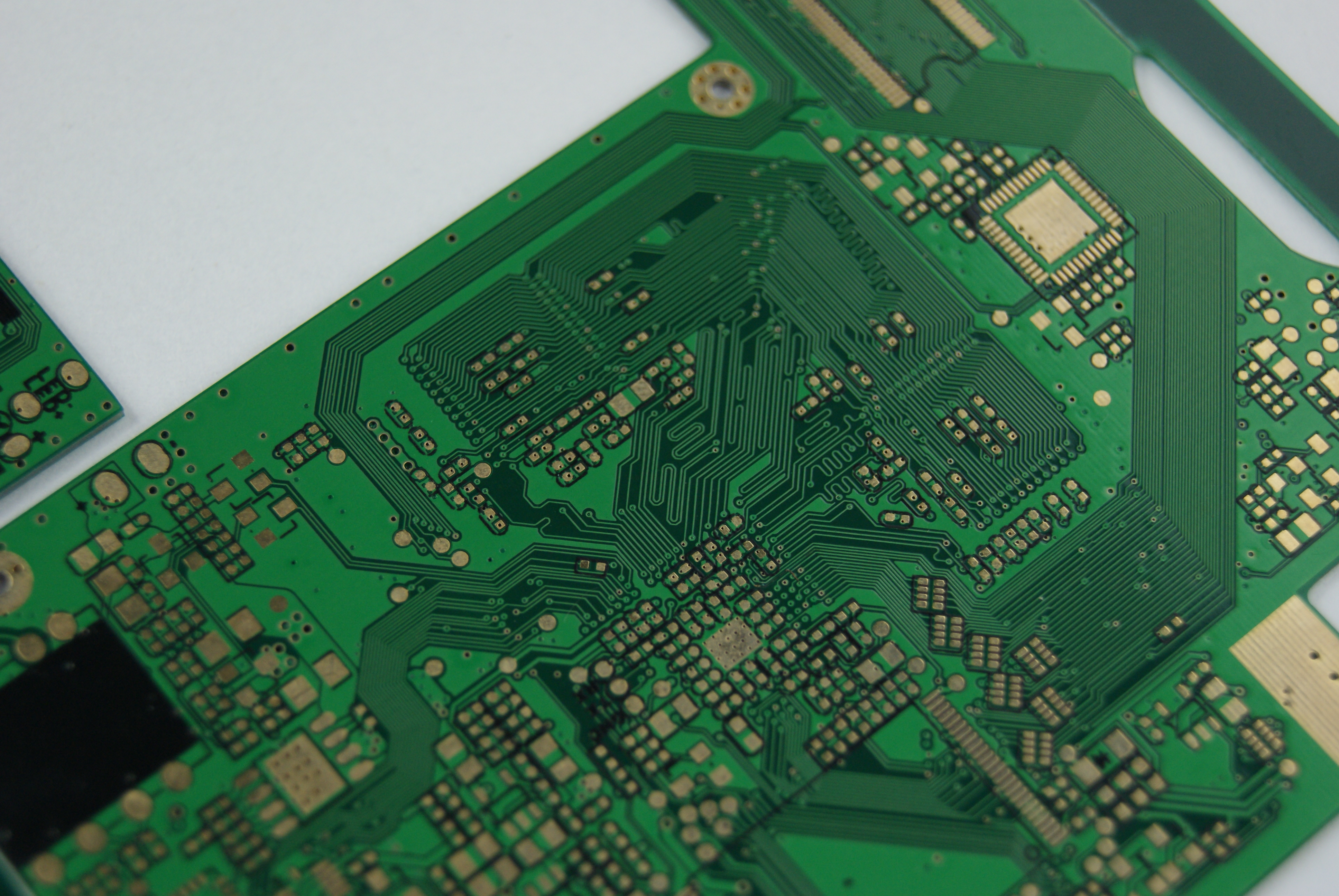
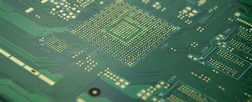
A multilayer PCB is a circuit board with three or more layers. These layers are joined with insulating materials to make them compact. Unlike single or double-layer boards, they fit more circuits in less space. This makes them important for devices like phones, medical tools, and cars.
To build a multilayer PCB, layers are stacked on top of each other. Inner layers manage power and signals, while outer layers connect parts. This setup blocks interference, reduces noise, and improves signal quality. Some multilayer PCBs can have up to 40 layers, using special materials for better performance.
How Does a Multilayer PCB Work?
Multilayer PCBs save space and reduce interference. Each layer has a job. Power and ground layers keep voltage steady and cut noise. Signal layers send data, and small holes called vias link the layers. The layers are aligned carefully to make a strong and compact board.
This design allows more parts to fit in small spaces. It also keeps signals clear by blocking noise. Multilayer PCBs are key for devices needing fast and reliable data transfer.
Key Parts of a Multilayer PCB
Conductive Layers
These copper layers carry power and signals across the board. The number of layers can go from 4 to 40, based on the design.
Prepreg Layers
Prepreg layers are insulating materials that hold the copper layers together. They keep the board strong and stop electrical problems between layers.
Vias (Blind and Buried Holes)
Vias are tiny holes that link the layers of the PCB. Blind vias connect outer and inner layers, while buried vias link only inner layers. These help make the board smaller and work better.
Advantages of Multilayer PCBs
Compact and Lightweight Design
Multilayer PCBs are important for modern electronics. Their small size helps fit more circuits into tiny devices. This makes them perfect for gadgets like phones and smartwatches. By stacking layers, these PCBs shrink the size and weight of systems while keeping them functional.
Feature | Benefit |
|---|---|
Compact Size | Makes devices smaller and easier to carry. |
Lightweight Design | Lowers device weight for better portability. |
High Circuit Density | Fits complex circuits in less space. |
This design meets the need for smaller, stronger devices. Multilayer PCBs allow high circuit density, keeping devices efficient and easy to use.
High Performance and Reliability
Multilayer PCBs work well and last long, even in tough conditions. They use strong materials like FR-4 and polyimide for stability. These PCBs also manage heat well, stopping parts from overheating or breaking.
Main reasons for reliability:
Heat-resistant materials handle high temperatures.
Low expansion reduces stress on soldered parts.
Careful manufacturing ensures steady performance.
Multilayer PCBs are trusted in industries like cars and planes, where reliability is very important.
Enhanced Signal Integrity and Functionality
Multilayer PCBs send signals clearly by cutting down noise and interference. Their layers include special ground and power planes, improving signal quality. This design ensures fast and clear data transfer, even at high speeds.
Advantage | Description | Impact |
|---|---|---|
Controls impedance to avoid signal loss and noise. | Fast and reliable signal transfer. | |
Improved Signal Quality | Ground and power layers reduce interference. | Clear signals for sensitive uses. |
Flexible Design | Extra layers allow advanced circuits and features. | Helps create compact and smart devices. |
These features let multilayer PCBs power devices with great performance and advanced features.
Manufacturing Multilayer PCBs
Key Steps in the Process
Lamination
Lamination is an important step in making multilayer PCBs. It stacks copper and prepreg layers into one board. The layers are lined up carefully for proper connections. High heat and pressure bond the layers tightly together. This process makes the board strong for complex circuits. Lamination keeps the PCB durable for tough uses like cars and telecom systems.
Via Formation (Including Blind and Buried Holes)
Vias are tiny holes that link PCB layers together. In this step, holes are drilled into the laminated board. Blind vias join outer and inner layers, while buried vias connect only inner layers. These holes save space and improve how the board works. After drilling, vias are coated with conductive material for electrical links. This step helps signals move smoothly between layers.
Etching and Plating
Etching removes extra copper, leaving the needed circuit paths. A protective layer, called photoresist, is added to the copper. Chemicals then dissolve the unwanted copper. After etching, plating adds a thin metal layer like gold or nickel. This improves conductivity and stops corrosion. This step ensures the PCB works well for modern devices.
Quality Control and Testing
Quality checks are very important for multilayer PCBs. Each board is tested to ensure it works properly. Visual and X-ray checks find problems like cracks or dirt. Automated optical inspection (AOI) spots assembly mistakes. Solder tests check if parts attach correctly. Standards like IPC-A-610 and ISO 9001 guide these tests. These steps are key for industries needing reliable PCBs, like telecom and automation.
Multilayer PCBs are vital for 5G and smart factories. They handle high-speed signals and power well, making them essential for today’s technology.
Multilayer PCB Applications
Consumer Electronics
Smartphones, Tablets, and Wearables
Multilayer PCBs are key parts of everyday electronics. They are found in phones, tablets, and wearables you use daily. These PCBs help fit more features into smaller devices. For example, phones need them for fast processors, great cameras, and strong batteries. Tablets and wearables also use them for touchscreens, fitness tracking, and wireless features.
The need for small, powerful gadgets is growing fast. This demand is pushing the market to grow from $28.66 billion in 2023 to $38.57 billion by 2032. The yearly growth rate is 3.36%. People want smart devices with many features, driving this increase.
Telecommunications
Networking Equipment and 5G Technology
Telecommunications depend on multilayer PCBs to work well. They are used in routers, switches, and base stations for fast data speeds. These PCBs are also crucial for building 5G networks. Without them, 5G’s faster speeds and better networks wouldn’t be possible.
This industry needs PCBs to handle high-speed communication. They cut down noise and keep signals clear. As 5G grows, more advanced PCBs will be needed. This will lead to new ideas and better designs in the future.
Medical Devices
Diagnostic and Implantable Devices
Multilayer PCBs are changing healthcare with better medical tools. Machines like MRIs and portable ultrasounds rely on them for accuracy. Small devices like pacemakers and hearing aids also use these PCBs. They make life-saving tools small and reliable.
The demand for new medical technology is rising. Multilayer PCBs are perfect for handling complex circuits in tiny spaces. They are strong and dependable, even in critical medical uses.
Multilayer PCBs are important for many devices, from gadgets to medical tools. Their flexibility and usefulness make them a must-have in today’s tech world.
Automotive and Aerospace
Advanced Driver Assistance Systems (ADAS) and Avionics
Multilayer PCBs are very important in cars and planes. In cars, ADAS uses these PCBs for smart features. These include collision alerts, lane-keeping, and cruise control. Multilayer PCBs are small and reliable, perfect for these tasks. They handle fast signals, making ADAS work well and safely.
Electric and self-driving cars need more advanced PCBs. These cars use them for power, sensors, and communication. Multilayer PCBs save space and keep performance high. This makes them great for modern vehicle designs.
In planes, multilayer PCBs are used in avionics and navigation. These systems must work in tough conditions. Multilayer PCBs protect against heat and stress, ensuring reliability. They are used in flight controls, radar, and communication tools.
Planes also need smaller, lighter parts to save fuel. Multilayer PCBs help by fitting complex circuits into tiny spaces. This improves efficiency without losing functionality.
Why these industries use multilayer PCBs:
Electric cars need them for power and sensors.
Planes rely on them for tough environments.
High-density PCBs meet strict aerospace needs.
Multilayer PCBs help cars and planes stay safe, efficient, and advanced.
Multilayer PCBs are key to making advanced electronic devices. Their small size and ability to handle complex circuits are crucial. They are widely used in cars, telecom, and airplanes. These PCBs allow for flexible designs with dense parts and clear signals. This makes them perfect for fast data transfer in modern gadgets.
Electric cars and smart driving systems need more multilayer PCBs. The growth of 5G networks also depends on these PCBs. They help manage high-speed signals for better communication. Using good design methods ensures these PCBs work well and last long. Multilayer PCBs keep improving electronics, making devices smarter and faster.
Multilayer PCBs are the heart of today’s technology, powering smart tools and fast communication systems.
FAQ
What makes multilayer PCBs unique compared to single-layer PCBs?
Multilayer PCBs have many conductive layers stacked together. Single-layer PCBs only have one layer. Multilayer PCBs can handle more complex circuits. They save space and work better. These are used in advanced devices like phones and medical tools.
How many layers can a multilayer PCB include?
Multilayer PCBs can have 4 to 40 layers. The number of layers depends on the device's needs. Complex systems like servers or aerospace tools need more layers. This supports advanced features and better performance.
Why are vias important in multilayer PCBs?
Vias link the layers in a multilayer PCB. They let signals and power move between layers. Blind and buried vias save space and improve how the board works. These are key for small and fast devices.
Are multilayer PCBs pricier than single-layer PCBs?
Yes, multilayer PCBs cost more because they are harder to make. But their small size, better performance, and reliability make them worth it. They are great for advanced electronics.
Can multilayer PCBs handle high heat?
Multilayer PCBs use materials like FR-4 and polyimide. These materials resist heat well. This makes them good for cars and planes, where durability is needed.
Tip: Pick the right PCB material for your device's environment. This ensures it lasts longer and works better.