Improving Multilayer PCB Reliability by Optimizing Conductive Traces
You can make multilayer PCB more reliable by improving conductive traces. This helps you get better signal quality, better heat control, and fewer problems.
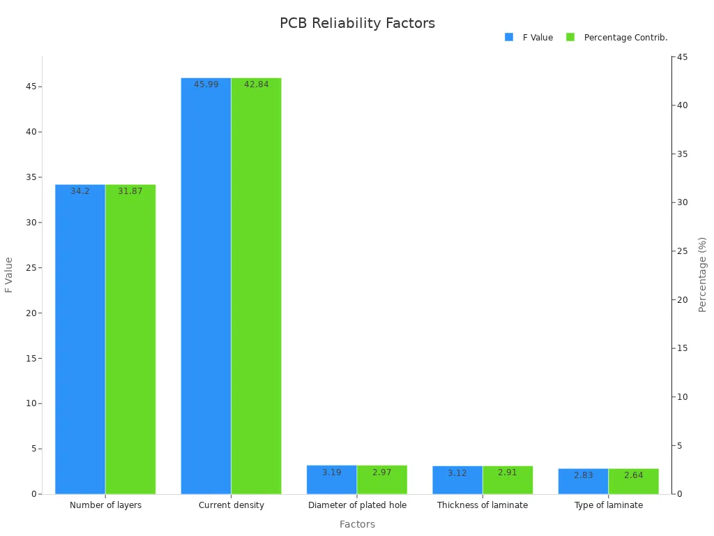
F Value | Percentage Contribution (%) | |
|---|---|---|
Number of layers | 34.20 | 31.87 |
Current density | 45.99 | 42.84 |
Diameter of plated hole | 3.19 | 2.97 |
Thickness of laminate | 3.12 | 2.91 |
Type of laminate | 2.83 | 2.64 |
LT CIRCUIT uses new materials and smart ways to design. They do this to meet these needs in every project.
Key Takeaways
Use IPC-2152 rules to pick the right trace width and spacing. This stops too much heat, signal loss, and electrical issues. It helps your PCB stay safe and work well.
Plan your layer stack-up and via design with care. This helps control heat and keeps signals clear. Use thermal vias, solid ground planes, and enough vias for better cooling and less noise.
Talk with your PCB maker early in the design. Tell them your goals and use simulation tools to find problems early. Working together makes strong and long-lasting multilayer PCBs.
Conductive Traces in Multilayer PCBs
Making conductive traces better is a key way to make multilayer PCB last longer. Rules like IPC-2152 tell you how wide and thick traces should be. These rules also say how far apart traces need to be. If you follow these rules, your PCB will not get too hot or lose signals. This also helps stop electrical problems. When you use these standards, your PCB is safer and works better.
LT CIRCUIT uses new ways to build PCBs. Their team knows how to make traces that carry lots of current. They also know how to stop crosstalk and control heat. You get good results for fast data, RF circuits, and power electronics.
Trace Width and Spacing
You must pick the right trace width for each signal and power line. IPC-2152 gives you advice based on current, copper thickness, and heat. For example, a 10A trace inside the board should be about 3.5 mm wide with 35 µm copper. This stops it from getting too hot. Traces on the outside can be thinner because they cool faster. You also need to keep enough space between traces. This stops arcing and crosstalk. For low voltage, keep at least 0.13 mm between traces. For high voltage, make the gap 2.5 mm or more.
Parameter | Typical Value Range (Based on IPC-2152) | Design Implication |
|---|---|---|
Trace Width for 10A (internal) | ~3.5 mm (35 µm copper, 10°C rise) | Prevents overheating in high-current internal traces |
Trace Width for 10A (external) | ~1.5 mm (35 µm copper, 10°C rise) | Surface traces dissipate heat more efficiently |
Minimum Clearance for ≤30V | At least 0.13 mm | Prevents arcing in low-voltage sections |
Minimum Clearance for ≥300V | 2.5 mm (basic), 5.0 mm (reinforced) | Required for high-voltage isolation |
Copper Thickness Options | 35 µm (1 oz), 70 µm (2 oz), 105 µm (3 oz), etc. | Impacts current capacity and thermal resistance |
If you make trace spacing bigger, signals stay strong at high frequencies. For low frequency, use 3 mils. For high frequency, use up to 8 mils. Guard traces that are 5 to 15 mils wide help stop crosstalk. Using the right resistors at the ends of traces keeps signals clear and lowers mistakes.
Case studies show that better trace design can cut crosstalk by half. Data stays clearer and timing errors go down by up to 30% in cars and RF designs when you follow these rules.
Layer Stack-Up
How you stack layers changes how signals and heat move. You must plan where signal, power, and ground layers go. A good stack-up lowers noise and helps heat move away. It also keeps signals strong. Studies show that different stack-ups, like memory-on-logic or logic-on-memory, change how heat and signals move.
Cadence research says that 3D stacking and more metal in layers can lower top temperatures and help cooling.
ScienceDirect tests show that more layers make heat harder to manage, but water cooling can help.
More ground and power planes in your stack-up give signals better paths and lower EMI.
LT CIRCUIT helps you pick the best stack-up for your project. Their engineers use computer tools to test different setups. You get a PCB that balances good signals and heat control.
Via Design
Vias link traces between layers. Good via design helps current flow and makes the PCB last longer. One small via can carry about 0.5 A. If you need more current, use more vias or bigger, filled vias. For a 10A path, use at least 20 small vias or a few big, copper-filled vias.
Tools like ANSYS and Altium Designer help you check current and heat in vias.
Bad via design can cause problems, even if traces are wide enough.
Microvias help heat move away and make high-power circuits more reliable.
LT CIRCUIT uses special ways to fill and connect vias. This helps heat move out and lowers the chance of failure. Their methods help you avoid problems and keep your PCB working in tough places.
Tip: Always talk to your PCB maker early. This helps you pick the right trace widths, stack-up, and via types for your project.
Best Practices for Reliability
Impedance Control
You must control impedance to keep signals clear and fast. Impedance means how much a trace stops electrical signals. If impedance does not match, signals can bounce back. This can cause errors. You should use controlled impedance routing. Keep traces the same width and distance from ground planes. This helps stop crosstalk and timing problems.
Simulation tools let you check impedance before building your board. These tools show how trace width, layer stack-up, or dielectric material changes signal quality. For example, field solver software shows how impedance shifts. It changes when you add layers or make the laminate thicker. Many engineers use these tools to keep impedance within 5% of the target. This helps your board work well at high speeds.
LT CIRCUIT uses advanced simulation and testing. They make sure your conductive traces meet strict impedance standards. Their team uses high-quality materials. They check every board with electrical tests. This keeps signals strong and products reliable.
Tip: Talk to your PCB maker early. Share your design goals. Get advice on trace width, spacing, and stack-up. This helps control impedance from the start.
Thermal Management
Good thermal management keeps your PCB cool and working longer. Heat builds up in power parts and can hurt conductive traces. You need to plan for heat. Use thermal vias, copper planes, and special materials to move heat away.
For example, put thermal vias under power chips. This helps heat flow to other layers. Copper planes can spread heat and lower hot spots by 22°C. Pick materials that handle heat well, like Rogers 4835, where temperature changes a lot. If a part gives off more than 2 watts, you may need a small fan for cooling.
LT CIRCUIT uses computer models to test how heat moves. They use thermal cameras and stress tests on real boards. Their engineers help you pick the right materials and layout for cooling.
Key thermal tips:
Keep via aspect ratios below 10:1 for strong plating.
Use thermal vias with 0.3mm holes and 1:8 aspect ratios under hot parts.
Adjust trace spacing by 25% in hot zones.
Test with both simulations and real measurements.
Ground Planes
Ground planes are big copper areas that give signals a safe path back. They help lower noise and keep signals clean. Use solid, unbroken ground planes under signal traces. This lowers EMI and makes signals better.
Stitching vias connect ground planes across layers. Put these vias close together, especially near fast signals. This keeps return paths short and lowers signal problems. You can also use ground planes to help spread heat.
LT CIRCUIT designs boards with strong ground planes and smart via placement. Their engineers use simulation tools to check for EMI and signal issues before making the board.
Note: Keep ground planes as solid as you can. Do not split them. Splitting can cause signal loops and extra noise.
Avoiding Common Pitfalls
Many PCB problems come from simple mistakes. You can avoid these by following a few key steps:
Plan your layer stack-up with care. Put power and ground planes between signal layers to cut down on interference.
Choose the right materials for your board. Look at thermal and electrical properties, not just cost.
Use the right type and number of vias. Too many vias can weaken signals and raise costs.
Test your design with prototypes. Use Automated Optical Inspection (AOI), X-ray, and stress tests to find problems early.
Document your design and changes. Good records help everyone on your team stay on track.
Work closely with your PCB maker. Early talks help you pick the best options for manufacturability and reliability.
Case studies show that poor layout, bad thermal planning, and not testing enough can cause failures. For example, a motor drive circuit failed EMI tests because of long traces and not enough decoupling. A power supply overheated because parts were too close and heat could not escape. You can learn from these mistakes by following best practices and using advanced testing.
LT CIRCUIT has top industry certifications like ISO 9001, UL, and IPC-A-600. They use AOI, X-ray, and environmental tests to check every board. Their team helps you avoid common mistakes and build reliable products.
Remember: Early teamwork, good records, and lots of testing are your best tools for reliable conductive traces and multilayer PCB success.
Making conductive traces better helps multilayer PCBs work well and last longer. You need to check your design with EVT samples. Test if it is strong enough for electricity and movement. Write down what you find in your tests. Work with your PCB partner, such as LT CIRCUIT, to pick good materials and control the process. Keep learning new things and improving your work to keep doing well.
FAQ
What is the best way to choose trace width for my PCB?
You should use IPC-2152 guidelines. Check your current needs and copper thickness. Ask your PCB manufacturer for advice if you are not sure.
How do ground planes help my multilayer PCB?
Ground planes give signals a safe return path. They lower noise and help keep your signals clean. You also get better heat spreading.
Tip: Solid ground planes work best. Avoid splitting them.
Why should I use simulation tools before making my PCB?
Simulation tools let you see signal and heat problems early. You can fix issues before you build your board. This saves time and money.
See Also
Challenges And Steps In Producing Multi-Layer Circuit Boards
A Comprehensive Guide To Manufacturing Multilayer PCBs
Step-By-Step Production Of Multilayer Rigid-Flex Boards