What is Package on Package Technology and How Does It Work
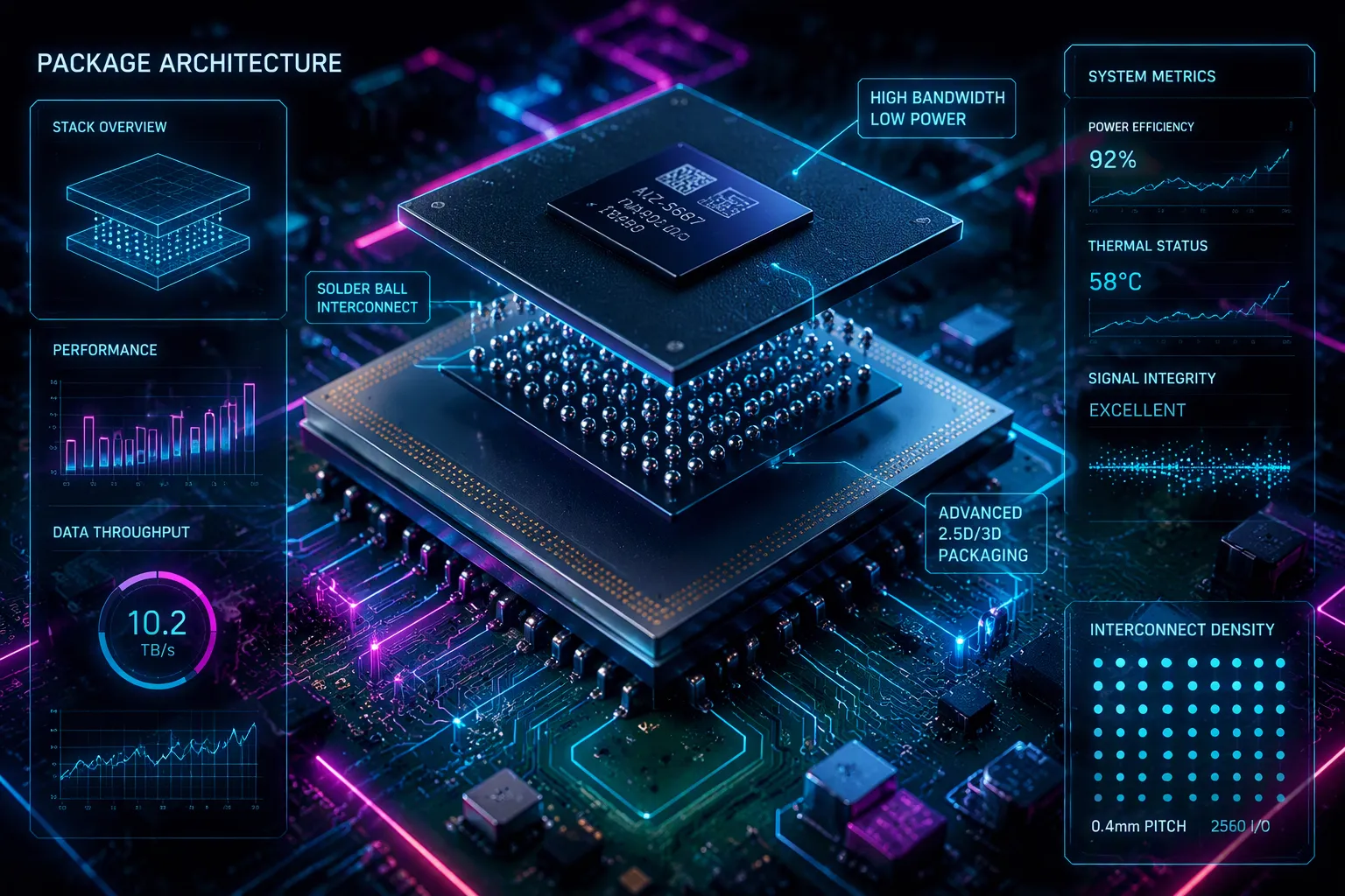
Package on package technology vertically stacks ball grid array (BGA) packages to maximize component density and save space on motherboards in compact devices like smartphones. This package on package (PoP) technology combines logic and memory chips in a single footprint. Analysts estimate the global PoP market in the multi-billion-dollar range, with an expected CAGR of 11.9% from 2026 to 2033. More than 70% of top-quality smartphones use multi-level memory-logic stacks, and over 70% of state-of-the-art mobile processors employ 3D/advanced stacking approaches such as PoP. You might ask yourself: how does this stacking and electrical connection actually work?
Key Takeaways
Package on package technology stacks memory directly above logic. This vertical design saves up to 50% of circuit board space.
Shorter signal paths between stacked chips speed up data transfer. Your device runs faster. It drains less battery power.
PoP combines a processor from one supplier with memory from another. This flexibility simplifies board design. It supports easy upgrades.
Smartphones use PoP to stack DRAM on application processors. This setup enables fast multitasking inside slim devices.
PoP technology powers wearables. It also powers IoT gadgets. It fits full computing power into tiny spaces.
Successful PoP assembly needs precise alignment. It also needs careful reflow soldering. These steps create strong electrical connections.
Engineers manage heat with thermal vias. They add heat spreaders. They apply interface materials. These methods keep stacked chips safe.
What is Package on Package Technology?
Defining Package on Package Technology
A Vertical Stacking Method for BGA Packages
Package on package technology vertically combines two or more ball grid array (BGA) packages into one compact unit. You place one finished package directly above another instead of arranging them side-by-side on the board. This approach to stacking multiple IC packages on top of each other separates PoP from 2.5D packaging, which places multiple naked dies side-by-side on a silicon interposer. Industry standards describe package on package as a 3D stacked packaging technology built for IC packaging and system integration in portable and mobile devices. The technique belongs to the broader field of advanced packaging, where engineers stack complete, individually encased chips during final PCB assembly.
Key Components: Logic and Memory
The key components of a PoP stack follow a consistent pattern. The bottom package usually holds a baseband or application processor, while the top package carries memory. This division lets you stack the processor and memory as separate units from different suppliers. Logic plus memory stacks commonly run 2–4 layers, and storage PoP designs can reach 8 layers. The pairing of processor and memory gives designers an effective 3D integration platform. It also simplifies supply-chain logistics, supports technology reuse, and allows large-scale customization.
You should not confuse PoP with flip chip. Flip chip is a die-level interconnect option used inside a package, where a die attaches face-down to the substrate through solder bumps. Package-on-package is a stacking method that connects complete packages vertically. A flip chip die can sit inside the base package of a PoP stack, so the two techniques complement each other rather than compete.
Aspect | PoP technology | Flip chip interconnection |
|---|---|---|
Packaging level | Package-stacking technology for 3D integration of logic with high-performance memory | Die-level interconnect used inside a package |
Typical structure | Molded FBGA base package with through-mold vias exposing PoP bond pads | Die attached face-down to the substrate with solder bumps |
Application driver | High-density memory stacking, reduced pitch, improved warpage control | Higher pin count and electrical performance in multi-core processors |
Relationship | Vertical stack of complete packages | Internal die-attach method inside the base package |
The Basic Structure
Top Package and Bottom Package
The basic PoP structure consists of two stacked modules. The bottom package contains the logic or processor. It sits on the motherboard through a high-density BGA, and its top surface provides landing pads for the upper package. The top package contains memory, such as DRAM or flash. It rests above the bottom package and connects to those landing pads through its own solder balls. In a standard PoP, the top package sits on the mold cap of the bottom package, and peripheral solder balls handle the electrical connections. In a through-mold via (TMV) PoP, vias pass through the bottom mold so the top package's solder balls sit partly inside the mold. That design produces a stable fine-pitch vertical stack.
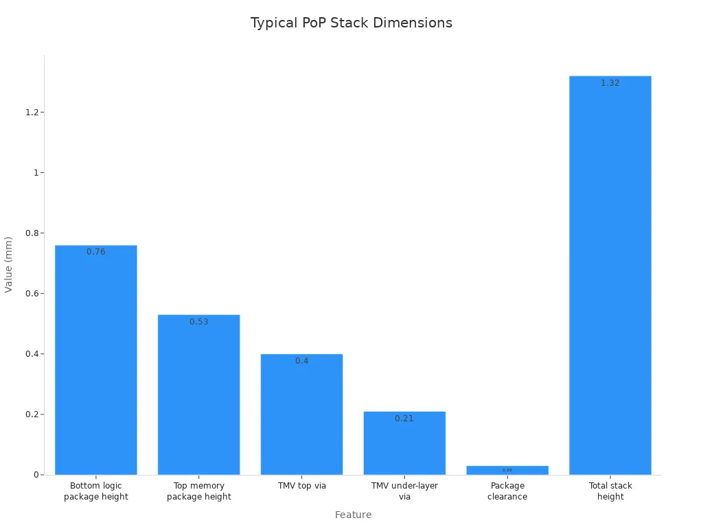
Typical dimensions show how tightly engineers pack these layers. A representative bottom logic package measures 0.76 mm in height, with a bottom BGA pitch of 0.4 mm and 620 pads. Its silicon die measures 7.10 × 6.97 × 0.13 mm. The top memory package measures 0.53 mm in height and connects through an upper solder array with 0.5 mm pitch and 200 pads. Through-mold vias measure 0.40 mm at the top and 0.21 mm at the under-layer. The overall stack fits a 14 × 14 mm footprint, leaves 0.03 mm clearance between packages, and reaches a total height of 1.32 mm.
Interconnection Through Solder Balls
Solder ball arrays interconnect the bottom-to-top package and the bottom-to-motherboard. The top package's BGA balls sit in the vias and contact conductive bumps on the bottom package. Assembly follows one of two main approaches. Pre-stacked PoP packages are assembled and reflowed as a single component. Alternatively, bottom and top BGAs are placed sequentially on the PCB and reflowed together. Both routes rely on precise solder ball alignment to guarantee reliable electrical connections across every layer of the stack.
How Package on Package Works
How PoP Technology Works
Stacking Process and Alignment
The PoP assembly process begins with the bottom package. You place this logic package onto the printed circuit board first, where its high-density BGA forms the foundation of the stack. Next, you dip the top package into flux or solder paste. This step coats each solder ball with the material needed for a strong joint. You then position the top package so every solder ball lands directly on its corresponding pad on the bottom package. The placement system must hold tight alignment for both packages, because PoP creates two soldering interfaces: top-to-bottom package and bottom-to-PCB. Any drift at either interface breaks the electrical path.
Alignment demands grow tighter as pitch shrinks. A representative bottom logic package uses a 0.4 mm bottom BGA pitch with 620 pads, while the top memory package connects through a 0.5 mm pitch array with 200 pads. These fine dimensions leave little room for error. After reflow, X-ray inspection verifies joint alignment and solder quality, confirming that precise solder ball contact was achieved across the entire array.
Reflow Soldering for Electrical Connections
The reflow soldering process bonds every layer at once. Heat melts the solder balls, which then cool and solidify into permanent joints. You can choose between two routes. Pre-stacked PoP packages arrive already assembled and reflow as a single component. Alternatively, you place the bottom and top BGAs sequentially on the PCB and reflow them together. Both routes depend on an accurate thermal profile. The profile must melt the solder completely without damaging the memory die or the logic die inside the stack.
Interconnection Methods
Solder Ball Grid Arrays (BGAs)
Solder ball grid arrays serve a dual purpose in every PoP stack. They provide mechanical support and establish electrical interconnections between the stacked packages and the printed circuit board. This vertical stacking approach lets you assemble multiple integrated circuit packages, such as a logic device or memory package with a processor, into one unit. The result reduces PCB area requirements and minimizes signal integrity issues while improving overall board performance. Each ball carries both power and data between layers, so a single weak joint can degrade the whole system.
Through-Silicon Vias in Advanced PoP
Advanced PoP designs replace peripheral solder balls with through-mold vias (TMVs). These vertical interconnects pass through the bottom mold so the top package's solder balls sit partly inside the mold. A TMV design produces a stable fine-pitch stack with better warpage control. In a representative stack, the vias measure 0.40 mm at the top and 0.21 mm at the under-layer. The overall assembly fits a 14 × 14 mm footprint and reaches a total height of 1.32 mm, with 0.03 mm clearance between packages.
Assembly and Testing
Ensuring Reliable Electrical Connections
Manufacturers test each package separately before stacking. Final assembly then requires its own inspection and testing to confirm reliability. Three procedures carry most of this load.
Testing Procedure | Purpose in PoP Assembly |
|---|---|
X-ray Inspection | Detects hidden solder-joint defects, including voids, especially between stacked packages where visual inspection is ineffective. |
Automated Optical Inspection (AOI) | Uses cameras to identify surface-level issues such as misplaced components, broken leads, or insufficient soldering. |
Electrical Testing | Verifies component functionality after inspection, often through in-circuit testing (ICT) or functional testing that simulates the device's operating environment. |
Specialized Rework Techniques
PoP rework requires specialized techniques to ensure reliable package stacking and electrical connections. The central challenge is selectively removing and replacing specific layers without affecting the other layers in the stack. You need PoP-capable rework systems with zero-force or near-zero-force removal so the lower package is not disturbed when the upper package is removed. Non-contact scavenging systems prepare the site consistently. Optical split-vision and precision BGA placement handle small, fine-pitch packages. For underfilled components, low-heat or no-heat removal tools such as lasers or milling machines protect the surrounding layers. You should also temporarily glue the bottom component to the PCB to prevent shift during reflow, and use dippable solder paste with high-activity fluxes for robust rework cycles. X-ray inspection with isometric viewing lets you check each solder-ball layer after the repair.
Why Use Package on Package (PoP) Technology?
Space Savings
Reducing Footprint on Circuit Boards
Package on package (PoP) technology delivers its most visible advantage through space efficiency. Stacking chips vertically shrinks the PCB footprint compared to side-by-side placement. That saved area gives you room for larger batteries, better cameras, or additional features inside the same device envelope. A side-by-side layout spreads chips horizontally and consumes far more board area. The PoP stack concentrates that real estate into a single compact module.
Enabling Thinner Devices
Height reduction matters just as much as footprint reduction in slim mobile designs. A typical PoP stack height drops, from 1.4 mm to 1.0 mm. The bottom package alone can shrink to less than 0.3 mm. These gains push the resulting overall PoP stack height as low as 0.8 mm. You gain thinner phones and wearables without sacrificing the processor and memory inside.
Performance Improvements
Shorter Signal Paths Between Components
Vertical integration places the processor and memory extremely close together. Short signal paths speed up data transfer between the logic die and the memory die. Side-by-side layouts use longer interconnects, which add delay and waste energy. The compact PoP arrangement keeps every connection brief and direct.
Enhanced Speed and Efficiency
Shorter paths reduce latency and lower power consumption. Your device runs faster while drawing less battery current. These core benefits of PoP technology matter most in mobile products, where thermal headroom and battery life are tight. The benefits of PoP extend beyond raw speed into everyday efficiency.
Design Flexibility
Mixing Different Chip Types
PoP supports heterogeneous integration. You can combine a logic package from one vendor with memory from another. A smartphone might pair a Qualcomm Snapdragon processor with 8GB of LPDDR5 RAM in a single compact module. Two common configurations exist:
Pure memory stacking: multiple memory-only packages stacked together.
Mixed logic-memory stacking: a logic package at the bottom with memory stacked on top.
The logic package sits at the bottom because it needs many more BGA connections to the motherboard.
Simplified Board Design
PoP lets you replace or upgrade a single chip, such as RAM, without touching the processor or motherboard. Smaller boards and fewer assembly steps reduce material and labor costs over time. Side-by-side designs need larger boards and longer interconnects. This modularity simplifies configuration changes and repairs across product lines.
PoP Technology Applications
Smartphones and Tablets
Combining Application Processors with Memory
Smartphones and tablets represent the largest market for PoP technology. Most flagship smartphones adopt PoP, stacking DRAM onto the application processor. This arrangement improves data access speed and supports multitasking. MediaTek builds several Dimensity processors with PoP. The Dimensity 8300 uses PoP for flagship smartphones. The Dimensity 9200 (MT6985W) pairs PoP with TSMC InFO-B. The Dimensity 9300 (MT6989W) uses PoP FCBGA with dimensions of 16.0 × 14.1 × 0.78 mm. The Dimensity 9500 (MT6993Z) combines a 3 nm process with Samsung LPDDR5X. Brands such as Vivo and OPPO deploy these chips in their flagship phones. You gain faster data transfer between the processor and memory inside one compact module.
Meeting Slim Design Requirements
Slim phone designs demand every component fit within tight height limits. A PoP stack places memory directly above the processor, so you save board area without adding thickness. This space efficiency lets manufacturers include larger batteries and advanced camera systems. However, heat generated within the mobile AP stays inside the DRAM, which can cause performance degradation. Engineers must balance thermal management against the compact form factor.
Wearable Devices
Smartwatches and Fitness Trackers
Wearables push miniaturization further than phones. A smartwatch packs processing, memory, and wireless connectivity into a case smaller than a matchbox. PoP technology enables this density by stacking memory chips on top of the processor. You get full computing capability inside a device that sits on your wrist. Fitness trackers follow the same pattern, using PoP to fit sensors and processing into slim bands.
Space-Constrained Designs
Every cubic millimeter counts in wearable design. A PoP stack reduces the PCB footprint compared to side-by-side placement. This saving gives you room for larger batteries or additional sensors. The vertical arrangement also shortens signal paths between the processor and memory, which lowers power consumption. Lower power means longer battery life for the user.
Other Electronics
Digital Cameras and Portable Media Players
PoP technology extends beyond phones into other portable electronics. Digital cameras use PoP to increase memory capacity and support multimedia functions. Portable media players stack memory on processors to handle audio and video processing. The same benefits of compact size and fast data access apply here.
PoP technology is described as a key enabler for feature-rich cell phones, with expectations that its use would spread beyond cell phones into digital still cameras and a wide range of multimedia applications.
Emerging IoT Devices
Internet of Things devices represent a growing application area. Networking equipment such as routers and switches use PoP to improve processing power and enable high-speed data transfer. As IoT devices shrink, the demand for compact packaging grows. You can expect PoP to play a larger role in this sector as devices become smarter and smaller.
Device Category | How PoP Is Used |
|---|---|
Smartphones and tablets | Memory chips are stacked on top of the application processor to improve data access speed and multitasking. |
Consumer electronics | Used in devices such as digital cameras and portable media players to increase memory capacity and support multimedia functions. |
Networking equipment | Applied in routers and switches to improve processing power and enable high-speed data transfer. |
PoP vs. Other Packaging Methods
PoP vs. System on Chip (SoC)
Integration Level Differences
A system on chip integrates all functions on a single silicon die. Package on package stacks separate dies into complete packages. The SoC approach demands a unified advanced process node for every function. PoP lets you pair a logic die with a memory die built on different nodes. You gain flexibility that a monolithic SoC cannot offer.
Cost and Flexibility Considerations
SoCs typically require higher upfront investment but achieve lower per-unit costs at high volumes. SiP solutions often provide lower initial development costs but may carry higher per-unit production costs. Cost trade-offs depend on your production volume expectations and market requirements. A high-volume flagship phone justifies SoC economics. A lower-volume device with mixed process needs favors PoP or SiP flexibility.
PoP vs. System in Package (SiP)
Stacking vs. Side-by-Side Placement
SiP integrates multiple independent dies within a single package. PoP is one vertical integration technique used within some SiP implementations. The two concepts are not equivalent. SiP is a system-level integration approach. PoP is a packaging and stacking technique. SiP can place dies side-by-side or in mixed arrangements. PoP specifically stacks complete packages vertically.
Use Case Scenarios
SiP supports mixed-manufacturing process integration, such as 28nm plus 65nm plus GaAs. This flexibility suits RF front-end modules, IoT devices, and wearables. PoP technology excels in applications needing tight processor-memory coupling, like smartphones. SiP can improve integration and footprint, but overall power consumption depends on individual dies, interconnect architecture, and thermal design rather than stacking alone.
PoP vs. Flip Chip
Stacking Method vs. Interconnect Method
Flip chip is a die-level interconnect option. It attaches a die face-down to the substrate through solder bumps. Package-on-package is a stacking method that connects complete packages vertically. A flip chip die can sit inside the base package of a PoP stack. The two techniques serve different roles in semiconductor packaging.
Complementary Roles in Advanced Packaging
You should not treat flip chip and PoP as competitors. Flip chip improves pin count and electrical performance inside a package. PoP technology adds vertical density across packages. Advanced designs combine both. A flip chip processor forms the bottom package, and a memory package stacks on top. This pairing delivers high performance in a compact footprint.
PoP Challenges and Limitations
PoP technology delivers impressive density, yet it also introduces serious trade-offs. You balance heat, precision, cost, and reliability against space savings.
Thermal Management
Heat Dissipation in Stacked Packages
Stacking dies vertically concentrates heat into a tiny area. A PoP stack confines the processor and memory inside one footprint. Heat reaches the PCB only through the C4, C5, and BGA solder interconnects. These bumps form a thermal bottleneck.
High currents and high temperatures cause electromigration. Metal atoms dislocate and form voids. These voids raise thermal resistance and current density. This combination accelerates electromigration and leads to device failure. Samsung's advanced packaging division counters this with thermal simulation, thermal-aware floor planning, and heat spreading structures. Their designs target high-density memory stacks.
Cooling Solutions
Thermal interface materials improve heat transfer between stacked layers. Heat spreaders move heat away from hot regions. Specialized substrate designs and advanced molding compounds create efficient conduction paths.
Through-silicon vias act as thermal conduits through the entire stack. Thermal vias and ground pads pull heat into the board. System-level cooling uses heat sinks, thermal pads, and airflow management. Integrated sensors feed dynamic algorithms. These algorithms adjust performance in real time.
Manufacturing Complexity
Precision Requirements
The assembly process requires exact alignment for every layer. You place the top package directly onto the landing pads. Pitch values near 0.4 mm leave no room for drift.
Warpage complicates the reflow step. Uneven heating bends the packages. Bent packages produce misalignment and cold joints. Larger stacks and thinner substrates make this problem worse.
Cost Implications
Precision equipment carries high costs. PoP technology requires high-end placement systems, x-ray inspection tools, and thermal profiling stations. Specialized rework systems add more expense.
Low volumes make PoP a poor fit. Side-by-side designs use cheaper standard equipment. PoP becomes economical when production volumes justify the capital investment.
Reliability Concerns
Mechanical Stress on Solder Joints
A PoP stack forms a tall, rigid structure. Solder balls carry electrical and mechanical loads. The bottom BGA supports the full weight of the upper package. Drops, flexing, and temperature swings concentrate stress at these joints.
Materials expand at different rates during thermal cycling. That mismatch strains the solder and forms cracks. Intermittent failures follow. The bottom layer suffers the highest stress. It bears the entire stack.
Testing Difficulties
You cannot visually inspect the inner solder joints between layers. X-ray inspection of a PoP detects voids and misalignment. This method requires expensive equipment and skilled operators.
Individual packages pass separate tests before stacking. Final assembly requires electrical testing of the complete PoP. This adds time and cost to production. A single hidden defect can compromise the whole device.
Package on package technology stacks BGA packages vertically. You assemble complete packages one above another. Solder balls create electrical connections between layers. Reflow soldering bonds the stack. Specialized rework methods handle repairs.
This package on package arrangement places memory directly over the processor. The package-on-package design shortens signal paths and shrinks the footprint. Smartphones depend on this structure for compact, high-performance builds.
TSMC allocated about $300M of its $1.5B advanced packaging CapEx in 2020 to InFO, a package on package (pop) technology platform. Apple adopted it for APUs in 2016. Ongoing assembly work confirms pop technology continues its evolution. Expect this technology to enter wearables and IoT gear next.
PoP continues to evolve and will likely migrate into other products further down the consumer-electronics food chain.
FAQ
What is package on package technology in simple terms?
Package on package technology stacks two or more ball grid array packages vertically into one compact unit. You place a memory package directly above a logic package. This arrangement saves board space and shortens signal paths between the processor and memory.
How does PoP differ from flip chip?
Flip chip is a die-level interconnect method. It attaches a bare die face-down to a substrate using solder bumps. Package on package is a stacking method that connects complete packages vertically. A flip chip die can sit inside the bottom package of a pop stack, so the two techniques work together.
Why do smartphones use PoP technology?
Smartphones need tight processor-memory coupling inside a slim body. PoP stacks DRAM directly on the application processor. This saves PCB footprint and shortens signal paths. You get faster data access and room for larger batteries.
What are the main challenges of PoP assembly?
Thermal management tops the list. Stacked dies concentrate heat into a tiny area, and solder bumps form a thermal bottleneck. Warpage during reflow causes misalignment. You also need expensive placement systems, x-ray inspection tools, and specialized rework equipment.
Can you rework a PoP package after assembly?
Yes, but rework demands specialized techniques. You need PoP-capable systems with near-zero-force removal to protect the lower package. Non-contact scavenging prepares the site. Optical split-vision handles fine-pitch placement. X-ray inspection with isometric viewing verifies each solder-ball layer after repair.
What is the difference between PoP and SiP?
SiP integrates multiple dies within a single package, often side-by-side. PoP specifically stacks complete packages vertically. SiP suits RF modules and IoT devices. PoP excels in applications needing tight processor-memory coupling, like smartphones and tablets.
How do through-mold vias improve PoP designs?
Through-mold vias pass through the bottom mold so the top package's solder balls sit partly inside. This design produces a stable fine-pitch stack with better warpage control. A representative stack fits a 14 × 14 mm footprint and reaches 1.32 mm total height.
What testing methods ensure PoP reliability?
Manufacturers test each package separately before stacking. Final assembly uses X-ray inspection to detect hidden solder-joint defects between layers. Automated optical inspection catches surface issues. Electrical testing verifies functionality through in-circuit or functional testing that simulates the operating environment.
