What Are Press-Fit Holes in PCB Boards
PCB boards with Press-fit Hole technology enable the connection of components without the need for soldering. This innovative press-fit method ensures robust mechanical and electrical connections, providing gas-tight seals, enhanced signal quality, and environmentally friendly assembly processes. These advantages make PCB boards with Press-fit Hole technology ideal for efficient and advanced manufacturing applications.
Key Takeaways
Press-fit holes create strong connections without soldering. They are great for modern PCB designs.
This technology reduces costs and is better for the environment. It also improves reliability and performance in many uses.
Choosing the right hole size and materials is important. This helps make PCBs last longer and work better.
Press-Fit Holes vs. Soldered Holes
Key Differences Between Press-Fit and Soldered Holes
Press-fit holes and soldered holes work differently and are made differently. Press-fit holes connect both mechanically and electrically. Soldered holes mainly focus on electrical connections. This makes press-fit holes more useful for modern PCB designs.
The way they are made is also different. Press-fit holes use a method like THT soldering but skip the solder. Soldered holes need a soldering step, which makes the process more complicated.
Here’s a simple comparison to explain:
Feature | Press-Fit Technology | Soldered Technology |
|---|---|---|
Connection Type | Electrical and mechanical connection | Mainly electrical connection |
Manufacturing Process | Like THT soldering, no solder needed | Needs soldering process |
Strength of Connection | Strong due to cold welding | Weaker mechanical connection |
Solder Usage | No solder used | Needs solder |
This table shows why press-fit holes are better for strong connections and easier assembly.
Advantages of Press-Fit Hole Technology
Press-fit hole technology has many benefits for PCB assembly. First, it doesn’t need solder, which lowers costs and helps the environment. Without solder, parts face less heat stress, making the product more reliable.
Another big advantage is the strong connection. Press-fit holes use an interference fit, creating a gas-tight seal. This seal makes the connection last longer and protects it from moisture and rust. This is great for products that need to work well for a long time.
Press-fit technology also makes manufacturing easier. Without soldering, production is faster and simpler. This is why industries like cars, telecom, and electronics use press-fit holes for large-scale production.
Choosing press-fit holes saves money, lasts longer, and is eco-friendly. These benefits make press-fit technology important for modern PCB manufacturing.
How Press-Fit Holes Work
The Mechanical Connection Process
Press-fit holes use a special mechanical process to make strong connections. Unlike soldered connections, they don’t need heat or solder. Instead, they rely on a tight fit, like "cold welding," to hold parts together.
Here’s how it works:
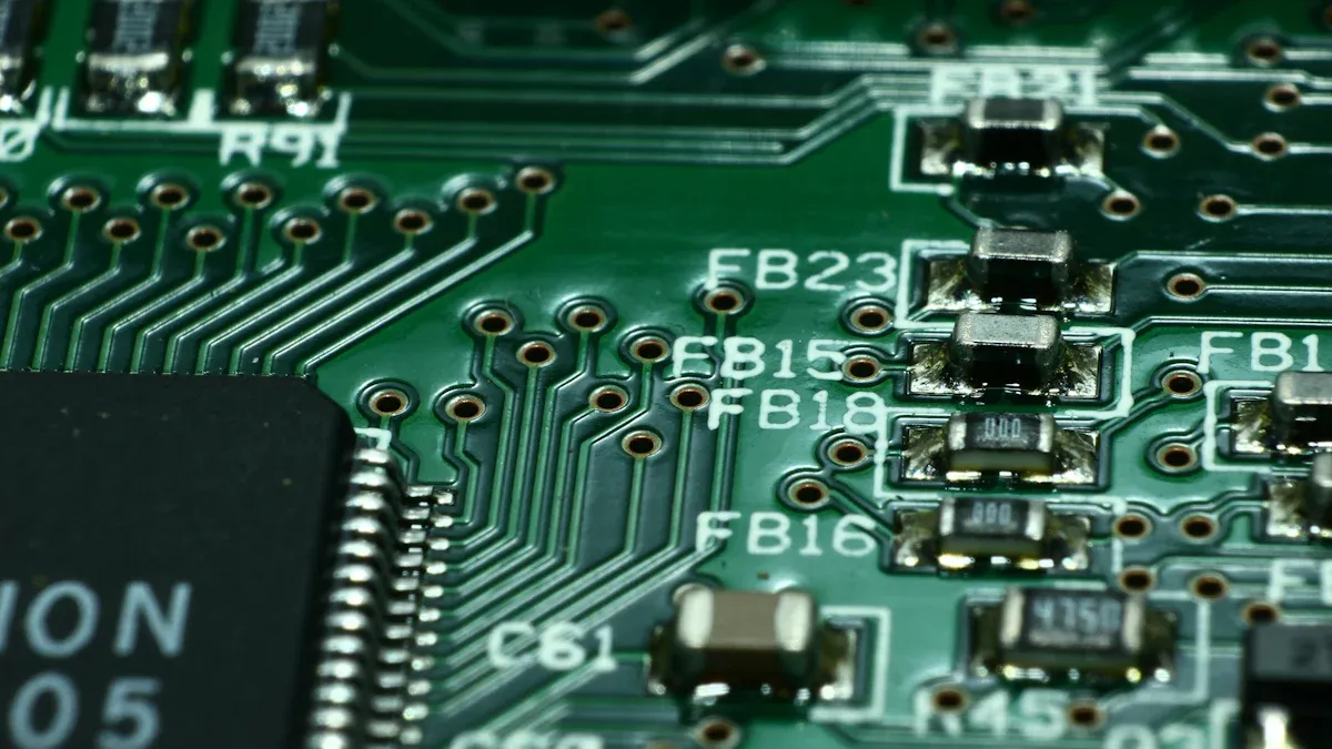
Drilling the Holes: Holes are drilled in the PCB to match the size of the press-fit parts. These holes are coated to allow electricity to flow.
Inserting the Pins: The pins are carefully pushed into the holes. Proper alignment is important to avoid damage to the PCB or parts.
Creating the Fit: When the pins go in, they form a tight seal. This seal ensures the connection is strong and allows electricity to pass through.
Older methods needed extra steps, like drilling both sides of the PCB and using tools. Newer methods, like friction riveting, skip these steps. They let you work from one side of the PCB, making the process faster and easier.
Role of Interference Fit in Press-Fit Technology
Press-fit technology works because of interference fit. This happens when the pin is slightly bigger than the hole. When the pin is inserted, the PCB material squeezes around it, creating a secure connection.
Here’s a breakdown of the process:
Description | |
|---|---|
Insertion and Retention Tests | Checks how much force is needed to insert and remove pins, ensuring the connection stays strong after repairs. |
Gas Tightness Tests | Tests electrical resistance to find cracks or weak spots after exposure to harmful gases. |
Cross-Sectioning | Examines how the hole and pin change shape during repairs to ensure quality. |
These steps make sure press-fit holes are durable and work well. The tight seal not only improves electrical flow but also protects against moisture and rust.
By using interference fit, press-fit holes avoid solder, reducing heat damage to parts. This makes them more reliable and perfect for jobs needing precision and strength.
Fabrication Process for a PCB Board with Press-Fit Hole
Drilling and Plating Steps
Making a PCB board with press-fit holes needs careful steps. First, the board is laminated. Then, holes are drilled where press-fit parts will go. These holes must be the right size to fit properly.
After drilling, the holes are cleaned to remove leftover debris. Next, a thin tin layer is added to the hole walls. This tin layer helps copper stick during plating. The board is dipped in a copper solution, replacing tin with copper. Electroplating adds more copper to make the holes strong and conductive.
These steps are important for making good PCB boards. They prepare the holes for press-fit parts to fit tightly and work well.
Importance of Hole Sizing and Tolerances
Hole size matters a lot for press-fit PCB boards. The parts need tight tolerances to fit securely. Usually, tolerances smaller than ±0.10mm are required to avoid loose fits or damage.
You must tell the PCB maker the exact tolerances needed. Most makers use a tolerance of ±0.004 inches. This ensures even the smallest holes fit the largest parts correctly.
Keeping tolerances precise helps the parts connect well. This makes the PCB last longer and work better with press-fit technology.
Design Tips for Press-Fit Holes
Picking Materials for PCBs and Connectors
Choosing the right materials is very important. The PCB must handle the stress from press-fit pins. FR4 is a common choice because it is strong and heat-resistant. For tougher jobs, materials like polyimide or Rogers laminates work better. These materials resist heat and improve electrical performance.
For connectors, the pin material matters a lot. Most pins are made of copper alloys. Copper is strong and conducts electricity well. To make pins last longer and stop rust, they are coated with tin, gold, or nickel. Always pick materials that work well together. This avoids problems like rust or bad electrical contact.
Keeping Tolerances for Press-Fit Holes
Exact measurements are key for good press-fit connections. The hole size must match the pin size closely. A tolerance of ±0.05 mm ensures a snug fit without harming the PCB. The hole’s shape must stay even from top to bottom. Uneven holes can weaken the connection or cause misalignment.
Here’s a table of important tolerance rules:
Specification | Requirement |
|---|---|
Hole Diameter | Matches pin size |
Hole Tolerance | |
Hole Cylindricity | Same size through the hole |
Hole Position | Matches land pattern |
Land Position | Lines up with holes |
Hole Perpendicularity | Drilled straight down |
Hole Axis Parallelism | Holes in a straight line |
Pin Size Tolerances | Looser than PCB hole tolerances |
Following these rules keeps press-fit connections strong and reliable, even in tough conditions.
Applications of Press-Fit Holes in PCBs
Use in High-Density PCBs
Press-fit holes are important for high-density PCBs. These boards need to fit many parts in small spaces. Press-fit technology helps by removing the need for soldering. Without solder, there’s more room for components. The tight fit keeps connections secure in crowded layouts. This makes press-fit holes perfect for modern devices like phones and laptops.
Using press-fit holes also makes high-density PCBs more reliable. The tight seal stops moisture and rust from damaging connections. This ensures the PCBs work well, even in tough conditions.
Applications in Automotive, Telecommunications, and Industrial Electronics
Press-fit holes are used in industries needing strong and precise PCBs. In cars, they provide safe connections for systems like engines and sensors. These PCBs handle vibrations, heat changes, and long use, making press-fit technology ideal.
In telecom, press-fit holes help with fast data transfer in routers and switches. The strong connections keep devices working well, even at high speeds. Industrial machines also use press-fit PCBs because they work in rough environments. Their sturdy design handles heavy tasks without breaking.
LT CIRCUIT’s Expertise in Press-Fit Hole Technology
LT CIRCUIT is a top expert in press-fit hole technology. They make PCBs with high-quality materials and advanced methods. Every press-fit hole is made with care and precision.
Whether you need PCBs for small designs or tough jobs, LT CIRCUIT delivers. Their focus on innovation and customer needs makes them a trusted choice. Choosing LT CIRCUIT means better PCBs that last longer and perform better.
Press-fit holes make building PCBs easier and more reliable. They allow faster production, save money, and create strong connections. The table below shows the main benefits:
Benefit | Explanation |
|---|---|
Easier assembly | Machines press in parts quickly. No soldering skills are needed. |
Better quality | Avoids solder problems like weak joints or bridges. Connections stay strong. |
Eco-friendly | No lead, fumes, or chemicals from soldering are used. |
LT CIRCUIT makes PCBs with care and accuracy. Their skill ensures top-quality products made just for you.
FAQ
What are the main benefits of press-fit holes in PCBs?
Press-fit holes make strong connections for parts and electricity. They don’t need soldering, which lowers heat damage and helps the environment. This makes them great for building reliable and efficient products.
Can press-fit holes handle high-density PCB designs?
Yes, press-fit holes are good for crowded PCB designs. They save space by skipping soldering and keep connections tight. This works well for small devices like phones and laptops.
Why is hole tolerance important in press-fit technology?
Exact hole sizes help pins fit tightly in PCB holes. This stops loose parts, makes the PCB last longer, and keeps it working well over time.
See Also
Achieving A Smoother Surface In HDI PCB Laser Drilling
Exploring The Manufacturing Steps For Rigid-Flex Circuit Boards
Understanding The Materials Used In Printed Circuit Boards