PCB Copper Thickness Selection Guide for 2026
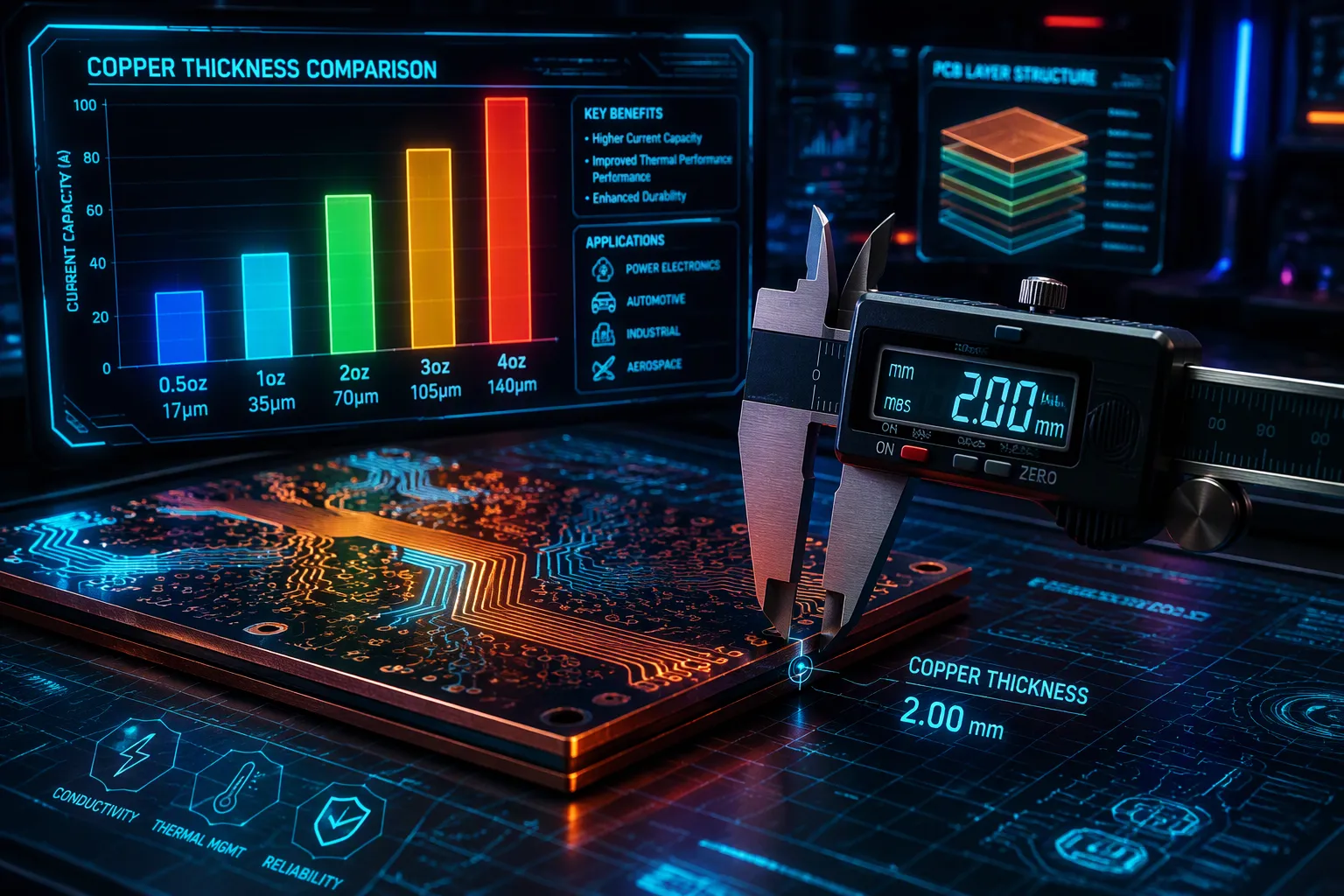
The right PCB Copper Thickness Selection depends on your needs for current, heat, strength, and cost. Most designs use 1 oz copper as the standard in the industry. Heavier copper works best for high-power or high-heat uses. When making your PCB Copper Thickness Selection, you must balance current capacity, heat control, mechanical strength, cost, and manufacturability. Traces that are too small get too hot, weaken over time, and can burn out. One case showed a 12 mil trace instead of 25 mils reached over 120 °C. Making traces too large raises cost and makes etching harder. You need the right PCB Copper Thickness Selection for reliable, affordable results.
Key Takeaways
Pick 1 oz copper for most regular boards to cut costs and make building easier.
For designs that are high-power or run hot, use heavier copper like 2 oz or more to improve performance.
When choosing copper thickness for your PCB, balance current, heat, strength, and cost.
Talk to your manufacturer early to make sure they can meet your copper thickness and trace width needs.
Follow standards like IPC-2221 or IPC-2152, and use calculators to check your design.
PCB Copper Thickness: Units and Standards
How Copper Weight Is Measured
The PCB industry measures copper thickness in ounces per square foot. One ounce of copper spread over one square foot is the standard unit. According to IPC-4562, 1 oz copper weighs 28.35 grams over 929 square centimeters. Copper density is 8.96 grams per cubic centimeter. This math gives about 34.1 microns. The nominal value in IPC-4562 is 1.37 mil, which is about 34.8 microns. In practice, you can treat it as 35 microns. A simple formula guides this conversion: thickness equals mass divided by area times density. Manufacturers often round to 35 microns, so both 34 and 35 show up in technical papers.
IPC-6012F lets you specify copper weight or thickness in microns. The standard prefers microns as the unit. Even so, industry practice still commonly uses ounces per square foot for copper thickness. You will see both units on datasheets and fabrication drawings. Knowing this dual system helps you talk clearly with your fabricator.
Common Values from 0.5 oz to 2 oz
You will run into several standard copper thickness values in PCB design. The most common copper thickness is 1 oz, which acts as the industry default. A copper thickness chart helps you compare options fast. The table below shows typical values.
Copper Weight | Thickness (µm) | Thickness (mil) |
|---|---|---|
0.5 oz | 17–18 | 0.7 |
1 oz | 34–35 | 1.35–1.4 |
2 oz | 68–70 | 2.7–2.8 |
The common copper thickness for PCBs goes from 0.5 oz to 2 oz. You should note that finished thickness after fabrication may differ from the starting foil. For example, 0.5 oz copper may measure 0.6 mils or 15 microns after processing. A 1 oz layer may end up at 1.2 mils or 30 microns. These changes matter for impedance control and current capacity. High-current designs often need 1–2 oz or more.
Key Factors in PCB Copper Thickness Selection
When you start a board, several forces shape your final choice. You must balance thermal, electrical, mechanical and manufacturing considerations together. Choose the right pcb copper thickness, and you control heat, strength, and cost at once. A small change in copper weight or thickness shifts all of these factors.
Current Capacity and Trace Width
Your first test begins with the load current. The current-carrying capacity of a trace depends on its width and the copper layer beneath it. IPC-2221 gives you a working relation. For 10 A at a 10°C rise, 1 oz copper requires a 2.5 mm wide trace. With 2 oz copper, the same 10 A needs only 1.2 mm. Another example reinforces the pattern. A 1 oz trace 5.2 mm wide carries 20 A at a 10°C rise. With 2 oz, the same current requires only 2.6 mm of width. You can also keep the width fixed and increase copper. A 1 oz trace 5 mm wide carries about 20 A, while a 2 oz trace of the same width carries about 28 A.
Voltage drop also drives your copper thickness and width selection. A 10-inch trace 1 mm wide has about 0.25 Ω at 1 oz. That resistance falls to 0.12 Ω at 2 oz. When you set current, thermal and voltage requirements, trace resistance matters as much as ampacity. Inner layers need wider traces because heat cannot escape easily. This lowers how much current a buried trace can handle. Plan inner layer widths against the same IPC-2221 curves. Budget for a smaller temperature rise instead.
Thermal, Mechanical, and Cost Trade-Offs
Thicker copper spreads heat better. A 2 oz copper plane moves heat about 30% more effectively than 1 oz. Hotspot temperatures can fall by 15–20°C. High-power LEDs on 2 oz copper can keep 10–15% longer life than on thinner standard foil. These gains support dense, high-power layouts. Thick copper also improves resistance to thermal-cycle fatigue. This protects solder joints and plated vias.
Mechanical strength rises as well. A 3 oz copper PCB is about 40% stiffer than a 1 oz board. Heavy copper pcb traces resist vibration cracking and pad wear from repeated connector insertions. Yet thick layers bend poorly. Thinner layers flex safely, while stiff heavy copper pcbs may crack under bending stress.
Cost moves against you. 2 oz copper costs about 15–20% more than 1 oz. Heavy copper pcbs at 3 oz or above can raise cost by 50% or more. Etching also gets more difficult. Longer etch times increase undercut risk and tighten minimum line/space limits.
Thicker ED copper improves current carrying capacity but increases etch difficulty and minimum line/space limitations, requiring tighter process control.
That tension defines heavy copper pcb design. You gain current and heat performance, but you pay for material and process time. For heavy copper pcb traces, plan wider spacing and accept lower resolution. Many designers reserve heavy copper pcbs for power stages and thermal zones. Your final choice should follow real load data, not a default habit. For ordinary boards, standard foil offers the best balance.
Current Capacity and Trace Width
Applying IPC-2221 and IPC-2152
You need a standard to size traces for current. IPC-2221 gives you a conservative formula from legacy tests. It usually covers copper up to about 3 oz. IPC-2152 takes a different path. It uses a universal nomograph with correction factors for board thickness, nearby copper planes, and internal versus external placement. That gap matters for heavy copper pcb designs. IPC-2152 supports copper up to 4 oz and beyond. It also accounts for how vias behave as thermal resistors in series with traces. The plated barrel often limits current, not the surface trace. Outer vias cool by convection, while inner vias trap heat. You can parallel multiple vias to raise capacity and spread heat.
How Copper Weight Changes Ampacity
Doubling copper weight from 1 oz to 2 oz boosts current-carrying capacity by about 100% for a 10 mil trace. That trace goes from 1 A to 2 A at a 10°C rise. A 50 mil trace rises from 2.6 A to 4.8 A, an increase of about 85%. These numbers come from IPC-2221 ampacity data for standard FR-4.
You can use this relationship to avoid oversizing. A trace width calculator helps you check current and copper thickness together. For heavy copper pcbs, the gain is real but not linear. Wider traces see less benefit than narrow ones. Heavy copper pcb traces also need wider spacing because etching gets harder. Always confirm your copper thickness/width choice against real load data. The right copper thickness and trace width balance ampacity, heat, and cost.
Thermal Management and Heavy Copper PCB
Copper as a Heat Spreader
When you plan a board, heat shapes your layer choice. A thicker heavy copper pcb lowers resistance in traces, pads, and vias. Less resistance means lower voltage drop and less heat made under the same current. Copper also holds heat. Like a thick towel cleaning a spill, a thick layer soaks up more thermal energy before it warms. This thermal inertia slows the rise in temperature. That margin matters for short overloads.
Doubling copper thickness from 1 oz to 2 oz can cut the lateral thermal resistance in the plane in half. For many boards, this pcb copper thickness can lower hotspot temperature by 15–25 °C. Wider copper planes spread heat to the board edge. Heavy copper pcb traces also carry current with less voltage drop. Thicker copper lets top-layer pads push heat toward the board surface. Lower resistance moves that heat well away from the junction. You get a cooler board without redesigning the enclosure.
When to Move Beyond 2 oz
You should move beyond 2 oz when a power plane or trace carries current that standard copper cannot handle. Heavy copper pcb weight starts above 3 oz per square foot. Heavy copper pcb designs often reach 6 oz or more for power uses. Power distribution layers use these weights to carry currents greater than 1 oz designs allow. On-board planar transformers also need heavy copper pcb construction. For currents above 5 A, increase clearance to other conductors. Keep at least 2 mm, or 80 mil, between heavy copper pcb traces to stop arcing.
Copper weights above 2 oz push standard fabrication limits. You must widen spacing and accept slower etch times. These costs make heavy copper pcbs an option for specific zones, not entire boards. Save heavy copper pcb for power stages, thermal areas, and transformer windings. Ground planes benefit, too. With careful layout, thick copper pcbs can replace outside heat sinks. Heavy copper pcbs also resist vibration and protect plated vias. Use heavy copper pcbs only where the thermal benefit is worth the price.
Mechanical Strength and Reliability
Stiffness, Vibration, and Flex Applications
Thicker copper makes a board harder to bend. A heavy copper pcb adds strength where connectors and plated holes attach. This lowers the chance of cracks during assembly or use. You will find this strength useful in cars and factory machines that shake all the time.
How stiff a board is depends on its thickness. Heavier boards resist bending and shaking better, so they work well in tough places. Large or thin boards warp more easily, especially during reflow soldering. Too much bending puts stress on solder joints and makes them less reliable. The right thickness keeps the board's shape stable while it is made and used.
Copper thickness directly impacts current-carrying capacity, thermal performance, and mechanical strength. Higher copper weights improve durability but also increase material cost and complexity in manufacturing.
Flexible and rigid-flex designs need a different plan. Trace shape should match the bending direction and how often it flexes. Smooth routing lowers stress in one spot, while sharp corners create hot spots. In dynamic flexing, route the copper pattern so repeated movement does not pile up strain in one place. Stiffeners and controlled bend transitions keep mechanical loads away from electrical connections. Making the board thinner does not always make it more reliable. A thinner build may flex more, but it also takes more damage from handling. You must think about substrate thickness, copper thickness, coverlay, and bend needs together. The smallest bend radius grows with layer count and copper weight. Tighter bends raise pulling stress on outer layers, which can crack conductors or break plating. Dynamic flex uses need bigger bend radii than static designs. Staggering traces across layers stops conductors from stacking right on top of each other, which would create stiff spots. Offset traces keep flexibility even and lower the risk of delamination.
Plating and Via Reliability
Via reliability depends on how thick and even the copper plating is. The plated barrel must survive z-axis expansion through every heat and cool cycle. Thin plating forms tiny cracks. Uneven plating puts stress at the weakest points. IPC-6012 sets the minimum average copper thickness for the hole wall.
Feature | Class 2 Minimum Average (µm/mil) | Class 3 Minimum Average (µm/mil) |
|---|---|---|
Hole Wall (PTH/Vias >2 layers) | 20 / 0.8 | 25 / 1.0 |
Surface Plating | 20 / 0.8 | 25 / 1.0 |
Microvia Cap Plating | Varies by table | 12 / 0.472 (min) |
A real failure shows why these limits matter. Class 3 boards failed thermal cycling tests. The average hole plating measured 18 µm, below the 25 µm threshold. Poor desmear caused weak seed adhesion. The insufficient copper thickness led to barrel cracks. The manufacturer fixed the process by extending permanganate etch times, which gave even and compliant copper thicknesses. You should check plating thickness with cross-sectioning and thermal cycling tests. Heavy copper pcbs with thicker plating survive more cycles. Heavy copper pcb traces also handle repeated thermal expansion better. For heavy copper pcbs in high-reliability uses, confirm your fabricator meets IPC-6012 Class 3 limits before production.
Cost, Etching, and Manufacturability
Etching Constraints and Minimum Trace Width
Etching removes extra copper, and thicker layers take longer to work on. When the inner copper is thicker, etching takes more time because there is more material to remove. This longer time in the etchant can cause undercutting, where the chemical eats the sides of traces under the photoresist mask. A 5 mil trace may shrink to 4 mils or less, which can hurt signal quality or current capacity. Thicker copper also needs stronger etching chemicals or higher temperatures, which raises manufacturing costs and harms the environment.
Thinner copper is easier and faster to etch, so it allows finer traces and tighter spacing. Advanced processes can make traces as small as 2 mils with thinner copper. But thinner copper is easier to damage during etching if it is not tightly controlled. Over-etching can remove traces or create weak points. Manufacturers must balance copper thickness with etching abilities to get consistent results.
The table below shows typical minimum trace width and spacing limits for heavier copper.
Copper Weight | Typical Minimum Trace Width / Spacing | Notes |
|---|---|---|
2 oz | 7/7 mil | Generally acceptable for prototype boards |
2 oz | 4/4 mil | Available but at higher cost due to lower yields |
2 oz | 10 mil trace/space | Recommended by one PCB manufacturer in their FAQ |
2 oz | 10/10 mil | Pushing the limit for DIY toner transfer etching; overetching and wavy edges occur |
3 oz and above | Wider rules than 2 oz | May need increased spacing/width; no specific numbers given |
6 oz | 18 mil spacing | Example from a shop for high-current boards (150V, 35A) |
Copper thickness: Thicker copper boosts current-carrying capacity and thermal performance but makes etching and lamination harder. Doubling copper thickness from 1 oz to 2 oz can raise etching time and material costs by 20–40%. Use heavy copper (≥2 oz) only in power or high-temperature areas. For signal layers, 1 oz copper is usually enough. You can also use selective plating to thicken copper only in certain areas.
Finding the Right PCB Copper Thickness for Budget
Cost goes up fast with copper weight. More copper thickness means higher raw material costs. Etching thick copper takes longer and is harder, which leads to higher processing costs and yield problems. In general, a 4oz board can cost 30%–50% more than a 1oz board. You must balance performance needs with budget limits.
A mixed-layer design is very cost-effective. In multilayer boards, use 2oz or 3oz copper only for power layers or certain signal layers that carry high current. Leave other signal layers with standard 1oz copper thickness. This way, you get the benefits of heavy copper pcb performance where it matters most without paying for it everywhere.
Cost Impact: More copper thickness raises raw material costs. Etching thick copper takes longer and is harder, which leads to higher processing costs and yield problems. In general, a 4oz board can cost 30%–50% more than a 1oz board.
Best Practice: A mixed-layer design is very cost-effective. For example, in multilayer boards, use 2oz or 3oz copper only for power layers or certain signal layers that carry high current, while leaving other signal layers with standard 1oz copper thickness.
Follow these steps to control costs while meeting performance goals:
Define Application Needs: Prioritize high current, high speed, or space efficiency. For power uses, use 1–2 oz/ft² copper; for high-speed or HDI designs, think about 0.5–1 oz/ft².
Consult Fabrication Capabilities: Work with your manufacturer to learn their etching and plating limits and make sure they can reach the trace widths/spacing you need for your chosen copper thickness.
Consider Cost Implications: Thicker copper raises material and processing costs because of longer etching times and more complex plating. Balance performance needs with budget limits.
Test for Signal Integrity: Use simulation tools to model impedance and signal loss based on copper thickness, then adjust your design for high-frequency performance targets.
Account for Thermal Management: Thicker copper moves heat away better, which is key for parts that make heat. Make sure your thickness choice meets thermal needs.
Step-by-Step PCB Copper Thickness Selection
Define Current, Thermal, and Mechanical Targets
Start with real numbers, not guesses. Find the highest steady and peak current for every critical power trace. Power electronics often need 2 oz or heavier copper, while consumer devices usually use 1 oz to save cost. Set your allowed temperature rise next, and most boards target 10–20°C above the surrounding air. Calculate trace width to see if widening the trace can carry the current and avoid thicker copper. Check voltage drop on long power traces by finding resistance and the resulting drop. Evaluate heat needs from component heat, copper planes, thermal vias, airflow, and enclosure conditions. For high-speed interfaces, check impedance so the copper thickness fits the stack-up and targets. Heat and vibration in the field mean you need extra thickness margin, and frequency changes usable thickness too. At GHz speeds, skin effect limits useful conduction to a few microns. Layer count and stack-up affect choices. Inner layers may use 0.5 oz copper to ease drilling and lamination, while outer layers may use heavier weights. Write copper thickness specs clearly in fabrication notes and balance copper across layers with symmetric buildups to avoid warpage. Use heavier copper only on power nets, but keep 1 oz copper for signal layers. Add a plating allowance of 0.7–1 mil to outer layers after etching. Set finished thickness targets to IPC-6012 Class 2 or 3 as needed.
Apply Standards, Run Calculators, Validate with Fabricator
You need a clear, repeatable process from design to final sign-off. Use these steps:
Use IPC-2221 and IPC-2152 to calculate trace width. Base it on a temperature rise limit, usually 10–20°C.
Derate internal layers by about 50%. Inner layers cannot shed heat as well as outer layers.
Use a trace width calculator. Enter current, copper weight, temperature rise, and layer type. It gives the minimum trace width or current capacity.
Check the design with thermal simulation tools and current calculators before sending it to production.
Confirm the factory can meet your specs. Check copper thickness, minimum trace/space, via diameter, aspect ratio, heavy copper processing, plating thickness, and registration tolerance.
Optimize cost. Pick the cheapest option that still gives enough reliability and performance.
IPC-2152 uses nomographs and correction factors that cover inner vs. outer layers, copper thickness, and heat. This gives more accurate sizing than IPC-2221. Copper weight changes how much current a trace can carry. Thicker copper has a larger cross-section and can raise capacity by about 60–100% at the same temperature rise. Designers must list copper weight per layer in fabrication notes. They also need to check which IPC standard the calculator uses, since IPC-2152 may allow narrower but still safe traces than IPC-2221. Work with manufacturers early and give them clear stack-up drawings, copper weight per layer, and target temperature rise. A DFM review before production can catch features that are hard to make consistently. Confirm the manufacturer can handle the needed specs, including minimum trace and space, minimum finished hole and drill sizes, annular rings, copper-to-edge spacing, solder mask registration, board thickness and tolerance, controlled impedance, blind/buried/microvia structures, surface finishes, materials, and copper weights. Test prototypes to confirm your predictions and adjust for real-world differences. Set specs early in design software because this prevents later changes. J-STD-001 soldering rules favor standard copper weights, which helps solder wet consistently. Thermal vias and plane stitching can remove heat, so you do not need thicker copper alone. Heavier copper raises cost and lead time because plating takes longer and handling is harder. DFM rules set minimum widths based on copper weight, such as 10 mils for 2 oz traces. Your best pcb copper thickness comes from this careful process, not from habit.
Best Practices for Specifying PCB Copper Thickness
Adjust Trace Width, Spacing, and Copper Balancing
Wider traces and wider gaps are needed as copper gets heavier. Thicker copper takes longer to etch. The etching chemical eats into trace sides, making a trapezoid instead of a vertical wall. If the gaps are too tight, copper slivers can stay at the gap base. These slivers can cause shorts or reduce electrical spacing. Over-etching to clear tight spaces strips too much copper from traces.
Give yourself extra room for etch factor compensation. Etch factor is extra trace width added up front so thicker copper can be processed without losing the final trace size. Grouping circuits with slightly more spacing improves processing. Published minimum trace widths and spacing rules are absolute limits, not stable production targets. Add margin above the stated minimum. This absorbs normal variation, improves yields, and allows moving production to another approved factory. Copper should be balanced across the panel too. Uneven distribution makes plating thickness vary from center to edge.
Consult Your Manufacturer Early
Talk to your manufacturer before you finish any heavy copper PCB design. On an outer layer, "2 oz finished" may start from 1 oz base foil and build up through electroplating. Inner layers do not get a major plating step. So a 2 oz spec on inner and outer layers gives different current-carrying behavior than you expect. Heavy copper PCB traces also get a trapezoid shape from etching. A nominal 6 mil trace on 2 oz copper can deliver less cross-sectional area than DC resistance calculations assume.
Use standard formats to share your stackup early. Gerber files are 2D and hold no copper-thickness information. Put the stackup in fabrication drawings or a board stackup report. Export drawings as DXF files from your CAD or ECAD tool, then share them as PDFs. Clearly label every part, including copper thickness and tolerances. Before you finalize, check the stackup and impedance values in your design software. For heavy copper PCB work, check that the manufacturer's etch factor and minimum trace width match the copper weight. Heavy copper PCB panels are heavier and stiffer. This affects conveyor handling and raises warping risk during lamination and reflow. Heavy copper PCB designs may also need thermal relief changes because thick copper pulls soldering heat away from through-hole joints. Added processing steps push heavy copper PCB cost up, so match your choice to the manufacturer's capabilities. Find out heavy copper PCB limits on thin board thickness. A quick DFM review can catch these issues before production. Heavy copper PCB success depends on this early partnership.
Consideration | 1 oz Copper PCB | 2 oz Copper PCB |
|---|---|---|
Manufacturing | Easier to fabricate and etch | Requires specialized manufacturing capabilities |
Signal Integrity | Suitable for most standard applications | Ideal for high-power and high-current designs |
Impedance Control | Sufficient for most applications | Important for impedance-controlled designs |
Design Flexibility | Provides flexibility for trace routing and design changes | May limit flexibility due to increased copper thickness |
Cost | Generally more cost-effective | Higher cost; weigh against specific requirements |
Manufacturer Consultation | — | Consult manufacturer to understand capabilities and cost implications; align choice with their capabilities |
Common Mistakes to Avoid
Assuming 1 oz Always Works
Many designers think 1 oz copper works for every project. This belief leads to real problems. The most common copper thickness is fine for signal routing and low-power circuits. But high-current or high-heat designs need something heavier.
You will notice several issues when 1 oz copper cannot handle the load. Narrow traces get too hot because they are too thin to carry the current. The copper can pull away from the board under too much heat. Hot spots appear in boards with tightly packed parts. Components run hotter than their limit and fail early. Above 100 MHz, higher resistance and impedance mismatches hurt signal quality. Nearby traces interfere with each other when the gap is less than three times the trace width.
You must figure out current needs with a safety margin. Add thermal vias and copper pours when heat cannot get out. Save heavy copper pcb zones for power stages and thermal areas. Do not put heavy copper pcb material on signal layers. That choice makes traces wider and uses routing space for nothing.
Ignoring Fabrication Limits and Cost Creep
Not every fabricator can make thick copper boards. Many suppliers cannot promise good results for inner layers with 6oz or 8oz copper. Some will double the price instead. You must check what they can do before you finish your design.
Heavy copper pcbs bring process problems. Lamination is not just stacking foil. Bad resin fill leaves empty spaces between inner-layer copper and prepreg. Delamination happens next under thermal expansion. Etch compensation issues can make the real copper cross-section smaller than planned. Resistance may run about 15% above the design value. Warping can happen even with balanced stack-ups. Two boards rated at 4oz copper can differ by more than 10°C in temperature rise on the same current path.
Using more copper weight than needed makes etching harder and raw materials more costly. Match your pcb copper thickness to the real current needs. Use mixed-layer designs. Put heavy copper pcb only where high current flows. Keep signal layers at standard weight. Lock in your design early. Late changes mess up buying and production planning. They create waste and cause delays. A careful approach keeps costs down without losing reliability.
Your pcb copper thickness selection balances current, heat, strength, and cost needs. Most designs use 1 oz copper. Heavy copper pcb works well for high-power jobs. Heavy copper pcb spreads heat. Heavy copper pcb adds stiffness. Heavy copper pcb raises cost. Heavy copper pcb buyers must set targets first. Apply IPC-2221A calculations. De-rate inner layers to about 50%. Confirm limits with your fabricator. When specifying pcb copper thickness, start with requirements. Your pcb copper thickness choice matters. Heavy copper pcb tools in 2026 make thick layers easier. Heavy copper pcb discipline decides success. Heavy copper pcb zones belong on power layers. Heavy copper pcb material resists vibration.
FAQ
What copper weight should I choose for a standard board?
You should start with 1 oz copper for most designs. This weight handles signal routing and low-power circuits well. It also costs less and etches easily. Move to heavier copper only when your current, heat, or mechanical needs demand it.
How does heavy copper pcb help with heat?
A heavy copper pcb spreads heat across the board. Doubling copper thickness from 1 oz to 2 oz can cut lateral thermal resistance in half. This lowers hotspot temperatures by 15–25 °C. Your components run cooler and last longer.
Can I mix copper weights on one board?
Yes, you can. A mixed-layer design uses heavy copper pcb only on power layers. You keep signal layers at standard 1 oz weight. This approach gives you high-current performance where you need it. It also controls cost and etching difficulty.
What limits trace width on thick copper?
Etching takes longer as copper gets thicker. The chemical eats into trace sides and creates a trapezoid shape. A 5 mil trace may shrink to 4 mils or less. You must add extra spacing and width margin for heavy copper pcb designs.
When should I avoid heavy copper pcb?
You should skip heavy copper pcb for signal layers and low-power circuits. Thick copper raises material costs by 15–50% and slows production. It also limits routing flexibility. Save heavy copper pcb zones for power stages and thermal areas only.
Does via plating matter for reliability?
Yes, it matters a lot. IPC-6012 Class 3 requires 25 µm average copper on hole walls. Thin or uneven plating causes barrel cracks during thermal cycling. Heavy copper pcb builds with proper plating survive more heat and cool cycles.
How do I confirm my copper thickness choice?
You should define current, thermal, and mechanical targets first. Then apply IPC-2221 or IPC-2152 to size your traces. Run a trace width calculator to check ampacity. Finally, confirm your pcb copper thickness with your fabricator before production.
