Single-layer vs Double-layer vs Multi-layer PCB Design Basics
Understanding different PCB types helps you choose wisely in electronics design. If you know how each layer and material works, you can build devices that work well and last long. This knowledge is the base of PCB Design Basics and helps you make your project more successful.
Key Takeaways
Learn about three main PCB types: single-layer, double-layer, and multi-layer. Each type is used for different electronics needs.
Pick single-layer PCBs for simple projects. They cost less and are easy to make. These are good for basic devices.
Use double-layer PCBs if your project is more complex. They let you add more parts and improve signal paths. These work well for medium-level devices.
Choose multi-layer PCBs for advanced projects. They handle fast signals and complex designs. They cost more and are harder to make.
Decide which PCB to use based on your project. Think about how complex it is, the cost, and how well it needs to work. This helps you pick the best PCB for your electronics.
PCB Types Overview
Printed circuit boards have different types. Each type is special and used for different jobs in electronics. There are three main groups: single-layer, double-layer, and multi-layer PCBs. Knowing about these types is important for PCB Design Basics.
Tip: Many new devices use more than one PCB type. This helps balance cost, how well it works, and size.
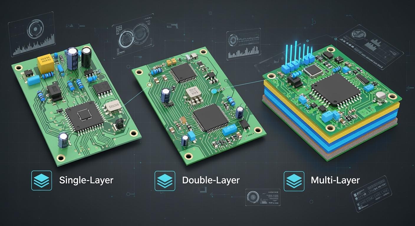
Single-layer PCB
Single-layer PCBs put all parts and circuits on one side. Makers use fiberglass or epoxy resin for the base. They add a copper layer for the circuit paths. A solder mask keeps the copper safe. A silkscreen shows where the parts go. This simple design makes single-layer PCBs easy to make and cheap. You can find them in calculators, LED lights, and simple toys.
Double-layer PCB
Double-layer PCBs have copper on both sides of the board. This lets you add more parts and make harder circuits. You can link both sides with small holes called vias. Double-layer PCBs are in many electronics like audio systems, TVs, cameras, and game consoles. You also see them in smart wristbands and power banks.
Multi-layer PCB
Multi-layer PCBs have many layers of copper and insulation. Most have four to twelve layers. Some special boards have even more. These boards are good for fast circuits and tricky designs. You find multi-layer PCBs in computers, servers, and strong devices. An 8-layer PCB can help move data fast and add cool features.
Note: Engineers pick multi-layer PCBs for high performance and small size.
Key Differences
Structure Comparison
You can see how single-layer, double-layer, and multi-layer PCBs are different by looking at how they are made. The number of copper layers and how they connect changes what each board can do. Here is a table that shows the structure and main features of each type:
Type of PCB | Characteristics | Advantages/Disadvantages |
|---|---|---|
Single-layer PCB | Conductive copper layer only on one side, suitable for basic circuit designs. | Lower cost, high manufacturing speed, easy to troubleshoot. |
Double-layer PCB | Conductive copper layer on both sides, suitable for complex circuit designs. | Higher cost, more flexibility in routing, but harder to repair. |
Multi-layer PCB | Several copper and insulating layers stacked together. | Best for complex, high-speed circuits, but costliest and hardest to repair. |
Single-layer PCBs have one copper layer. All parts and traces go on one side. Double-layer PCBs have copper on both sides. You can use vias to connect traces from one side to the other. Multi-layer PCBs stack four or more copper layers with insulation between them. This design lets you fit more circuits in a smaller space.
Tip: Multi-layer boards often use special layers for power and ground. This keeps signals clean and stable.
Functionality Comparison
How you use each PCB type depends on how many layers it has. The number of layers changes how you route signals, place parts, and handle complex designs.
Single-layer PCBs
These are good for simple circuits. You only have one layer for traces, so you must plan carefully. These boards work best for basic devices where you do not need many parts.Double-layer PCBs
You get more freedom with two copper layers. You can place more parts and make shorter connections. This helps improve signal quality and lets you build more complex circuits. Double-layer PCBs also handle moderate electromagnetic interference better than single-layer boards.Multi-layer PCBs
You can design very complex circuits with many layers. These boards let you route signals on different layers, which keeps them from interfering with each other. Multi-layer PCBs support high-speed signals and advanced features. You often see them in computers, servers, and other powerful devices.
Here are some key points about how layer count affects performance:
More layers help you route signals and keep them strong.
Multi-layer PCBs lower electromagnetic interference.
Higher layer counts support faster signals and more features.
For most products, starting with a four-layer board gives you a strong base. As your design grows, you may need six, eight, or more layers to keep up with performance and reliability needs. PCB Design Basics teaches you that the right layer count makes your board work better and last longer.
PCB Design Basics: Comparing Layers
Single-layer Advantages
Single-layer PCBs are easy to use and cheap. They work well for simple electronics and projects with few parts. Here is a table that lists the main good points:
Advantage | Description |
|---|---|
Low Cost | Single-layer PCBs cost less to make, about 30-50% cheaper than double-layer boards. |
Simplicity in Design | The simple design means fewer mistakes and faster making. |
Ease of Testing and Repair | You can see problems easily, which helps students and hobbyists fix them. |
Suitability for Low-Density Designs | Great for basic circuits with not many parts, so things do not get too hard. |
Faster Production Times | Fewer steps mean the boards are made faster, which helps if you need them quickly. |
Tip: If you want to learn PCB Design Basics, start with single-layer boards. They help you see how circuits work.
Single-layer Disadvantages
Single-layer PCBs cannot do everything. They do not work for hard or fast circuits. Here are some reasons why:
You cannot put lots of parts on one board.
The board cannot handle crowded or tricky designs.
No ground planes makes it hard to stop electromagnetic waves.
Fast signals do not move well, so you lose signal and control.
Making many boards is easy, but not very exact, which can hurt how well they work.
You should use single-layer PCBs only for easy projects. If you need more parts or better results, you should try other types.
Double-layer Advantages
Double-layer PCBs let you do more with your designs. You can put parts on both sides and link them with vias. This helps you make harder circuits. Here are some main benefits:
You can draw paths on both sides, so it is easier to connect things.
Signals move better because you can control their path.
More parts and features fit on the same board size.
These boards work better for medium-speed and more complex devices.
Double-sided PCBs let you control impedance for better signals, with about ±10% tolerance.
In double-sided boards, you can keep impedance close to 50 ohms for signal paths. Single-sided boards have less steady values.
Double-layer Disadvantages
Double-layer PCBs are harder to make than single-layer ones. You will have some problems when using them:
Making these boards is harder, so they cost more.
You need better tools and skills to design and fix them.
Soldering on both sides can cause mistakes, so you must be careful.
Extra steps like making holes and lining up both sides take more time.
Making these boards takes 20-30% longer than single-layer PCBs.
There are more mistakes, so checking quality is important.
If you want to use double-layer PCBs, plan for more steps and higher costs.
Multi-layer Advantages
Multi-layer PCBs give you the most options and power. You can use them for fast and crowded designs. Here are some reasons engineers pick them:
You can send signals on many layers, which keeps them strong and stops interference.
Multi-layer PCBs let you fit more parts and work better.
You can keep digital and analog signals apart, which helps performance.
Special power and ground layers help spread power and stop voltage drops.
Good planning lets you add more features in a small space.
More layers make signals better and cut down interference.
Multi-layer boards need careful planning for paths and lining up layers.
Note: PCB Design Basics says multi-layer boards are best for advanced things like computers and servers.
Multi-layer Disadvantages
Multi-layer PCBs also have some bad points. You should know these before picking them:
Making these boards costs more because they are hard to build and line up.
Fixing multi-layer PCBs is tough since you cannot reach inside layers.
Many problems cannot be seen without special tools.
These boards are often thrown away instead of fixed, especially if saving money matters.
More layers mean more chances for mistakes if layers do not line up or get hurt.
You must watch heat closely to keep the board working well.
If you want to use multi-layer PCBs, plan for higher costs and harder repairs. Only use them if you need fast, crowded, or special features.
Applications
Single-layer Use Cases
Single-layer PCBs are used in products with simple circuits. These boards are good when you want low cost and easy building. Many companies use them for basic electronics. For example:
Old radios use single-layer PCBs because their circuits are simple.
New LED lights use these boards for steady work.
You also see single-layer PCBs in toys, calculators, and small home gadgets. These boards help keep things simple and dependable.
Tip: If you make a school or hobby project, start with a single-layer PCB. You will learn the basics and avoid hard problems.
Double-layer Use Cases
Double-layer PCBs let you connect more parts together. You can use them in devices that need more features but not the complexity of multi-layer boards. Here is a table that shows where double-layer PCBs are used:
Device Type |
|---|
Printers |
HVAC Units |
Line Reactors |
Vending Machines |
Amplifiers |
You can find these boards in audio gear, office machines, and some home devices. Double-layer PCBs help you fit more parts in less space and make your device work better.
Multi-layer Use Cases
Multi-layer PCBs are used in advanced technology. You find them in devices that need fast data, strong signals, and many features. These boards are important in telecommunications and computers. For example, you see multi-layer PCBs in:
Networking devices
Routers
Switches
Smartphones, modems, and other small devices also use multi-layer PCBs to save space and work better. Also, these boards help with:
Signal transmission
GPS applications
Satellite applications
When you need high speed, small size, and strong performance, multi-layer PCBs are the best choice.
Performance Factors
Signal Integrity
Signal integrity is how well signals move through the PCB. The number of layers changes how signals travel. More layers help keep signals strong and clear. Look at the table below to see the differences:
PCB Type | Signal Integrity Benefits | Issues Addressed |
|---|---|---|
Single-layer | Limited routing options, higher crosstalk risk | Signal degradation |
Double-layer | Reduced noise through ground planes, more stable reference planes | Increased loop area, potential ringing |
Multi-layer | Improved routing, minimized crosstalk, dedicated ground/power planes for stability | EMI, voltage fluctuations, signal distortion |
Multi-layer PCBs let you keep signals apart. You can put signal and ground layers next to each other. This setup protects signals from outside noise. Ground and power planes keep voltage steady and lower electromagnetic interference (EMI). Double-layer PCBs use ground planes to cut noise, but they do not control impedance as well as multi-layer boards. Single-layer PCBs have fewer choices, so signals can get weak or mixed up.
Thermal Management
Heat can hurt your PCB if you do not handle it well. Multi-layer PCBs use tricks to move heat away from hot parts:
Thermal vias send heat down through the board to cooler layers.
Copper pours spread heat across the board like a big heat sink.
Heat sinks pull heat away from hot parts.
High thermal conductivity materials help heat leave faster.
Smart component placement puts hot parts where air can flow better.
For example, in electric vehicles, copper pours and heat sinks keep power parts cool. This helps the system stay safe and last longer.
Power Distribution
Power must reach every part of your PCB without causing trouble. Multi-layer PCBs do this best. They have special power and ground planes inside the board. These planes keep power steady and stop signal lines from picking up noise. Single-layer and double-layer PCBs run power and ground traces next to signal lines. This setup can cause power loss and signal problems. Multi-layer PCBs also work better in small devices and tough places. You get less electromagnetic interference and more reliable performance, but you pay more for these benefits.
Cost and Manufacturing
Material Costs
You need to think about material costs when you choose a PCB type. The number of layers changes how much you pay for each board. More layers mean more copper, more insulation, and more work. This makes the price go up. You can see the average costs for different PCB types in the table below:
PCB Type | Size (mm) | Cost per Unit ($) |
|---|---|---|
Double-Layer | 100 x 100 | 1 - 5 |
Multilayer (4) | 100 x 100 | 5 - 15 |
Multilayer (6) | 100 x 100 | 20 or more |
A double-layer PCB costs less than a multi-layer PCB. If you pick a 4-layer board, you pay more than double-layer, but less than a 6-layer board. When you add more layers, the price can rise quickly. You should match your budget to your project needs.
Tip: If your project is simple, a double-layer PCB can save you money.
Production Complexity
Production gets harder as you add more layers to your PCB. Simple boards need fewer steps. Multi-layer boards need special machines and more time. You must press and heat each layer together. If your design uses blind or buried vias, you add even more steps. Each lamination cycle can take 4 to 6 hours. This makes the whole process longer.
You also need to check each layer for mistakes. More layers mean more chances for errors. If something goes wrong, you may need to start over. This adds to the cost and time.
You should know that complex PCBs take longer to make and cost more. Plan your project timeline with this in mind.
Choosing the right PCB type helps you balance cost, speed, and quality. If you want fast production and low price, use fewer layers. If you need high performance, you may need to pay more and wait longer.
Choosing the Right PCB
Selection Criteria
You need to look at several factors before you pick a PCB type for your project. Each factor helps you decide which board fits your needs best. Here is a list that shows what you should check:
Size and Shape
The board’s size and shape affect how much material you use and how long it takes to make. Large or odd-shaped boards need more work.Complexity
If your circuit has many parts or special features, you may need more layers. Complex designs cost more and take longer.Type of Board
You can choose rigid, flexible, or rigid-flex boards. Each type works for different projects.Material
The base material changes how the board handles heat and strength. Some materials cost more but last longer.Layer Count
More layers help with complex circuits. They also raise the price and production time.Copper Thickness
Thick copper lets you run more power. It also adds to the cost.Surface Finish
Different finishes protect the board and change the price.Trace Width
Wide traces carry more current. They use more copper and cost more.Lead Time
If you need your board fast, you pay more.Custom Features
Special designs make the board harder to build and more expensive.Application Suitability
Make sure the PCB matches your project’s needs.Technical Specifications and Substrate Choice
Check the technical requirements and pick the right material.Quality and Manufacturing Standards
Look for boards that meet high quality standards.Customization and Prototyping Capabilities
See if you can customize or test your board before full production.Manufacturer’s Service and Delivery Capabilities
Choose a reliable manufacturer who can deliver on time.
Tip: Write down your project’s needs before you pick a PCB. This helps you match the board to your goals.
You can pick from different PCB types. Each one is good for certain jobs.
Type of PCB | Layers | Description | Applications |
|---|---|---|---|
1 | Easy design, all parts on one side | Simple electronics | |
Double-Sided PCB | 2 | Metal on both sides, more ways to connect | Medium-level devices |
Multi-Layer PCB | 3+ | Layers stacked for hard circuits | Advanced, packed electronics |
Think about how hard your project is, how much you can spend, and how well it should work.
Use single-layer boards for easy projects.
Double-sided boards are better for medium needs.
Multi-layer boards are best for tough jobs but cost more.
Before picking a PCB, do these things:
Know what you want your project to do.
Write down what your device must do.
Set goals for how well it should work.
Look at where your device will be used.
Plan how much money and time you have.
Make sure you follow any rules or get needed approvals.
Planning ahead helps you choose the best PCB and make strong electronics.
FAQ
What is the main difference between single-layer and multi-layer PCBs?
You see single-layer PCBs with only one copper layer. Multi-layer PCBs have several layers stacked together. Multi-layer boards handle complex circuits and high speeds. Single-layer boards work best for simple devices.
Can you repair a multi-layer PCB easily?
You find it hard to repair multi-layer PCBs. The inner layers stay hidden. You need special tools to fix problems. Most people replace these boards instead of repairing them.
Why do you choose a double-layer PCB for your project?
You pick double-layer PCBs when you need more parts and better signal paths. These boards let you connect both sides. You get more features without the high cost of multi-layer boards.
How does the number of layers affect PCB cost?
You pay more for each extra layer. Single-layer PCBs cost the least. Double-layer boards cost more. Multi-layer PCBs cost the most because they use more materials and need complex manufacturing.
See Also
Understanding The Differences Between PCB Types And Layers
Essential Skills For Designing Multilayer PCB Layouts Effectively
An In-Depth Look At The Multilayer PCB Manufacturing Process
Exploring The Diverse Applications Of Multilayer PCBs
Challenges In Manufacturing And Prototyping Multilayer Circuit Boards