Beginner’s Guide to a Complete PCB Design Checklist
You need a good pcb design checklist when you start your first pcb design. If you miss important steps, you might put parts in the wrong place. You could also have signal problems or expensive mistakes when making the board. Many new designers have trouble with noise, too much heat, or slow production. This guide shows you each step, so you can change the checklist for your project and stop common errors.
Consequence | Description |
|---|---|
Manufacturing issues | Not enough annular rings can break drills and cost more money. |
Incorrectly placed components | Putting parts in the wrong spot can make mistakes and short circuits. |
Signal interference | Signal bounce can cause crosstalk and make the board less reliable. |
Overheating risk | Too much current can make the board get too hot. |
Use your checklist to check every small thing. You make your circuit work better and feel more sure with each project.
Key Takeaways
Use a PCB design checklist to help you not make mistakes. This will also help your board work the right way.
Always check your schematic to stop problems like wrong connections and signal issues.
Look at component footprints and compare them with datasheets. This helps you stop prototype failures and put parts in the right place.
Plan for test points early in your design. This makes it easier to fix problems after you build the board.
Run Design Rule Checks (DRC) before you finish your design. This helps you find errors like short circuits and missing connections.
PCB Design Checklist Essentials
A good pcb design checklist is very important. It helps you finish your project without big mistakes. You need to follow each step so your board works right. This section shows the main steps for every beginner pcb design.
Schematic Verification
You begin your pcb project with a schematic. This drawing shows how parts connect. Many beginners skip this step, but it is very important. Most pcb problems happen during the schematic phase. If you do not check carefully, your board might not work.
Always check that the footprint matches the schematic symbol. Pin count and numbering must be correct, or you will have wrong connections.
Use your design software’s tools to check your work. These tools sort checks into groups. They help you find missing parts, wrong ratings, and pins that do not match.
Run Design Rule Checks (DRC) and Design for Manufacturability (DFM) checks. These checks find problems like not enough space or nets that are not connected.
Automated Optical Inspection (AOI) and In-Circuit Testing (ICT) help you find mistakes before you build the board.
Tip: Careful schematic review stops most errors. Take your time with this step in every tutorial or checklist.
Footprint and Packaging Checks
Wrong footprints cause many pcb prototype failures. You must check that every footprint matches the part’s datasheet. This step is very important for beginners.
Practice | Description |
|---|---|
Use Industry Standards | Follow IPC-7351B rules for pad sizes, clearances, and solder mask. Keep at least 10 mil (0.25 mm) space around each part. |
Run Design Rule Checks (DRC) | Set rules for trace width, spacing, and nets. For example, use a minimum trace width of 0.15 mm for standard boards. |
Peer Review | Ask someone else to check your footprints. Another person can find mistakes you miss. |
Make a Prototype | Build a prototype before making many boards. This step shows real problems like soldering defects or fit issues. |
You should also check for clear polarity markings and pin 1 signs. These markings help you and the manufacturer put parts in the right place. Always check copper-to-edge spacing and via sizes to meet manufacturing needs.
Component Placement Basics
Good component placement makes your pcb easier to build and more reliable. You should group parts by what they do. Put power chips close to the loads they serve. Keep decoupling capacitors near power pins. Beginners often forget to keep analog and digital sections apart, but this lowers noise.
Principle | Explanation |
|---|---|
Smart positioning | Put key parts like power chips close to loads and decoupling capacitors near power pins. |
Avoid obstacles | Keep screw holes and snap-in areas clear. Keep enough space from board edges. |
Group parts by what they do to make loop areas smaller.
Put heat-making parts near the board edge for better airflow.
Keep sensitive circuits away from noisy power parts.
Make a rough floor plan before you start. This plan helps you place connectors and other parts based on signal flow.
Good placement helps machines put and solder parts correctly. It keeps signal paths short, which protects signal quality and stops problems like delay.
Note: Careful placement at the start of your pcb design checklist saves time and stops mistakes later. Every tutorial and checklist should include this step.
By following these steps, you build a strong base for your pcb. Each step in your pcb design checklist helps you avoid common mistakes and makes your beginner pcb design process easier.
Routing and Constraint Rules
Trace Width and Clearance
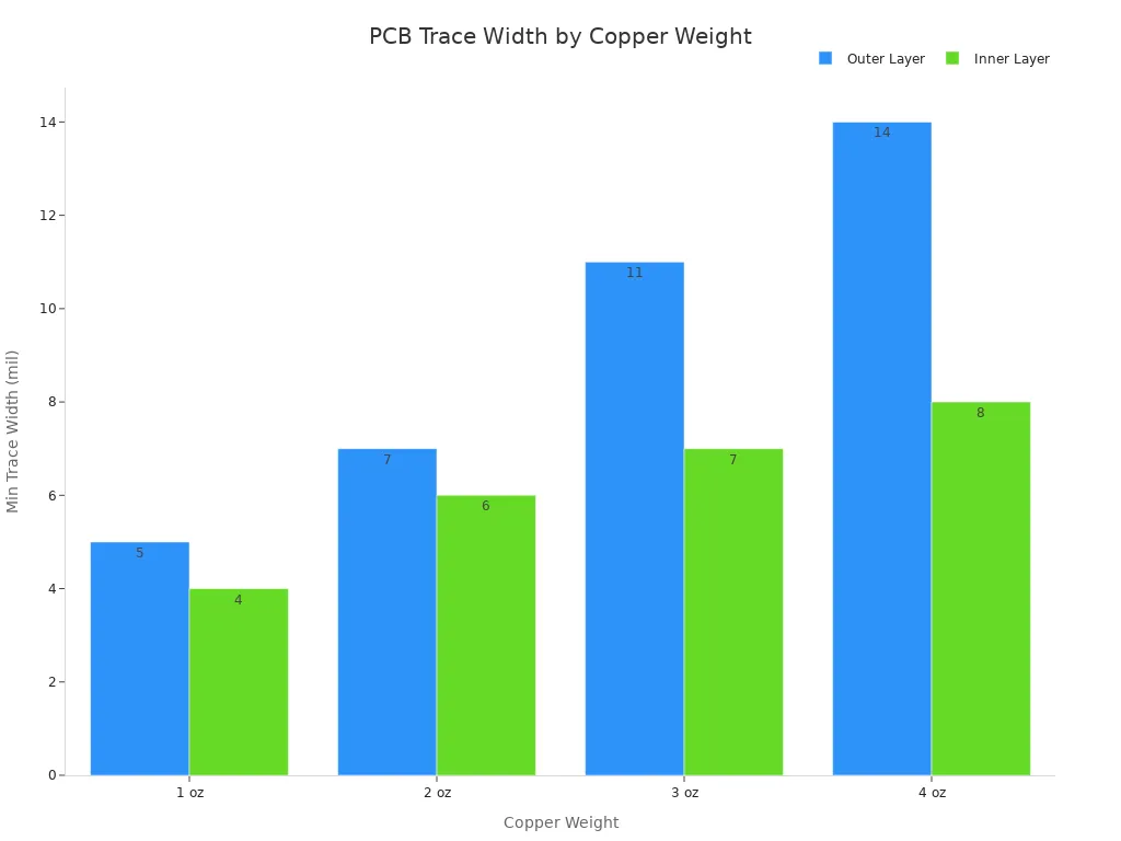
You need to pick the right trace width and clearance for your pcb. These choices keep your board safe and working well. Thin traces can get too hot or break. If traces are too close, you might get short circuits or sparks. The copper weight changes how wide your traces must be. Look at the table below for usual standards:
Copper Weight | Standard Minimum Trace Width | Advanced Minimum Trace Width |
|---|---|---|
0.5 oz | 3 mil (0.075mm) | 2.5 mil |
1 oz | 4 mil (0.1mm) | 3 mil |
2 oz | 6 mil (0.15mm) | 5 mil |
You also need enough space between traces. For 1 oz copper, keep at least 4-5 mils between traces. This space stops shorts and keeps signals clean. The chart below shows how trace width changes with copper weight and layer:
Tip: Always check your manufacturer’s rules in every tutorial before routing.
Signal Integrity Checks
Signal integrity means your signals move without getting messed up. In beginner pcb design, you might see problems like crosstalk, reflections, and jitter. Crosstalk happens when signals on nearby traces mix together. Reflections come from impedance mismatches and can change your signals. Jitter is a small timing error that can make data wrong.
You can use simulation tools to check signal integrity. Many tutorials suggest Cadence Sigrity, Ansys SIwave, or Altium Designer for this job. These tools help you find problems before you build your pcb.
Keep traces short and straight.
Do not run high-speed signals next to each other.
Use ground planes to protect sensitive signals.
Power and Ground Planes
Power and ground planes make your pcb stable and lower noise. You should use solid areas for ground planes. This design gives signals a safe path back and helps with heat. Put decoupling capacitors close to power pins. Use both small and big capacitors for best results.
Best Practice | Description |
|---|---|
Use separate ground planes when needed | Helps control noise and interference. |
Single-point grounding at power entry | Stops ground loops. |
Continuous ground planes for high-speed boards | Makes signal integrity better. |
Isolation gap ≥ 2 mm | Stops unwanted coupling. |
Avoid routing signals across zones | Keeps signal quality good. |
Note: Every tutorial should remind you to connect all ground points with short, wide lines. This step keeps your circuit steady and lowers noise.
If you follow these routing and constraint rules, your pcb will be more reliable and easier to make. Each tutorial you use will help you build better boards and stop common mistakes.
Design for Manufacturability (DFM)
Mechanical Integrity
You need to check if your pcb is strong before making it. Good solder joints and clean surfaces help your board last longer. Use the table below to help you check:
Mechanical Integrity Check | Description |
|---|---|
Solder Joint Fillet | Smooth, curved edges mean strong connections. Bumpy shapes can mean weak soldering. |
Solder Joint Shape | The right shape for each part helps your board handle stress. |
Solder Joint Cleanliness | Clean joints stop rust and short circuits. |
Solder Joint Strength | Joints must be tough. Cracks show weak spots. |
Cleaning Requirements | Clean boards work better and last longer after being made. |
Hot oil tests can show if your pcb can take heat. This test finds weak solder joints and bad materials.
Always check these things in every tutorial to stop problems when building your board.
Solder Mask and Silkscreen
You must design the solder mask and silkscreen layers carefully. The solder mask covers traces and keeps solder in the right place. Make sure the solder mask is at least 2 mil bigger than each copper pad. Keep a 1 mil ring around pads. For green and red masks, use at least 4 mil web thickness. Other colors need 5 mil.
The silkscreen should not cover pads, vias, or parts. This step stops soldering problems.
Use text that is at least 25 mil tall for silkscreen. This size makes labels easy to read.
Good solder mask and silkscreen design make building easier and lower mistakes. Every tutorial should tell you to check these layers.
Panelization Considerations
Panelization lets you make more than one pcb at once. You can put many boards together on one panel. This step saves time and money. It also helps you get more boards and waste less material.
Benefit | Impact on Cost and Yield |
|---|---|
Reduced Setup Times | Cuts assembly time by up to half |
Minimized Labor Costs | Lowers handling time and human mistakes |
Increased Board Yield | Better layouts can give you 20% more boards |
Material Waste Reduction | Uses standard laminate sizes better |
Increased Efficiency | Lowers scrap and helps make more good boards |
You should always follow spacing rules, check drill sizes, and look at part clearances. These steps help you avoid expensive mistakes in beginner pcb design. Every tutorial you use should have DFM checks to make sure your pcb is easy to build and works well.
Design Review Checklist
A strong design review checklist helps you find mistakes early. You should use this checklist for every beginner pcb design. It keeps your project moving and helps you learn from each tutorial.
Rule Check (DRC)
You must run a Design Rule Check (DRC) before you finish your pcb. This step finds errors like short circuits or missing connections. It also finds spacing problems. DRC tools in your design software show you where to fix things. You should check for:
The right trace width and enough space between traces
Correct pad sizes and via sizes
No nets that overlap or are missing
A good pcb design review also checks test points, high-voltage spacing, and panel setup. The table below shows some important things to check:
Category | Checklist Item |
|---|---|
Testing | Test pads away from the board edge, no stubs on fast nets, easy to reach for testing |
Protection/EMI/EMC | Creepage and clearance rules, ESD paths, direct routes for fast signals |
Panels | Enough frame area, panel fiducials, right panel size for thickness and cutting |
Tip: Always use your design review checklist to double-check these rules in every tutorial.
BOM and Documentation
A complete Bill of Materials (BOM) and clear documents make your pcb easy to build and test. You should list all details for each part. This helps you, your team, and your manufacturer avoid mix-ups.
Here are the main things to put in your BOM:
Item number for each part
How many of each part per board
Manufacturer part number (MPN)
DNI/DNP (Do Not Install/Populate) status
Reference designator
Vendor name (optional)
Vendor part number (optional)
Value (optional)
Size or footprint
Part description or specs
You should also add package type, placement method, board layer, and notes. Good documents help every tutorial and make your pcb design review faster.
Final Design Review
The final design review is your last step before you send your pcb for production. You should check for common problems that beginners face. These include missing signals, wrong part rotation, and incomplete netlists. The table below lists some problems and how to fix them:
Issue Type | Specific Problems | How to Fix |
|---|---|---|
Schematic Design | No access signal on pins | Set I/O on pins |
Parts outside the drawing area | Move parts to the right spot | |
Partial access from netlist | Make sure global nets are included | |
Parts do not rotate | Change how you enter the part | |
PCB Layout | Network loading errors | Check if any packages are missing |
DRC shows split networks | Use copper to connect everything | |
Large file size or blue screen | Export files in smaller groups |
You should always use your design review checklist and follow each tutorial closely. This habit helps you avoid costly mistakes and build better pcb projects.
Testing and Quality Assurance for Beginners
Test Points and Accessibility
You should plan test points early in your pcb project. Test points help you check if your board works after it is made. Many beginners forget this step, but it makes fixing problems easier. Put test points close to important nets like power and ground. Spread them out across the pcb so you can reach them with probes. Use pads that are big enough for test tools. Do not put test points on important signal paths because it can cause interference. Mark all test points clearly in your design files and on the silkscreen. In crowded circuits, use staggered test points to save space. Always leave enough room for probes so you do not hurt the board when testing.
Put test points near important nets.
Mark test points so they are easy to see.
Use big pads for easy testing.
Spread test points out across the board.
Do not let test points mess up signal paths.
Tip: A good pcb quality checklist always has test point planning.
Simulation and Functionality
Simulation tools let you test your pcb before you build it. You can use these tools to find problems like signal delays or overheating. This step saves money and helps you avoid mistakes. Simulation shows how signals move over long traces. You can look at graphs and waveforms to understand your circuit better. Running simulations helps you make sure your design works well and meets standards. This process lets you fix weak spots before you build the real board. For beginners, simulation builds confidence and helps you learn how circuits work.
Common Beginner Mistakes
Beginners often make the same mistakes in pcb design. You might forget to add enough test points or put them where they are hard to reach. If you skip simulation, you can miss problems. Not using a pcb quality checklist makes errors more likely. You may use the wrong pad sizes or forget to mark test points. These mistakes make testing and fixing harder. Always check your design for these problems before sending your pcb for production.
Mistake | How to Avoid |
|---|---|
Not enough test points | Plan and mark all test points |
No simulation | Run simulations before production |
Bad pad sizing | Use big, easy-to-test pads |
No checklist | Follow a pcb quality checklist |
Remember: Careful testing and quality checks help beginners build reliable pcbs every time.
EMI/EMC and Protection
Electromagnetic interference (EMI) and electromagnetic compatibility (EMC) are important for a reliable pcb. You need to know where EMI comes from and how to stop it. EMI in beginner pcb projects often comes from fast signals, switching circuits, ground loops, cables, and bad layout. Fast signals and clock circuits can act like antennas and spread noise. Switching power supplies and impedance mismatches can make EMI worse.
Shielding and Filtering
You can lower EMI in your pcb by using shielding and filtering. Shielding uses grounded metal boxes or copper shields to cover sensitive parts. This makes a Faraday cage and blocks noise. It can cut radiated EMI by up to 40 dB. Put decoupling capacitors close to IC power and ground pins. These capacitors help keep noise low and lower loop inductance. Filtering parts like ferrite beads and LC filters stop EMI on power lines and I/O. Shielded cables and grounded connectors also help lower noise.
Use grounded shields to protect sensitive parts.
Put decoupling capacitors near power pins.
Add EMI filters at power and I/O connectors.
Use ferrite beads or LC filters on power lines.
Tip: Good signal routing and keeping traces close together help lower noise in your pcb.
ESD and Overcurrent Protection
You need to protect your pcb from electrostatic discharge (ESD) and too much current. ESD can break important parts if you do not use protection. Find out where ESD can hit and add ways to stop it. Common protection parts are transient voltage suppressor diodes, reverse bias Zener diodes, varistors, and fuses. You can also use voltage-sensing relays, gas discharge tubes, crowbar circuits, and MOSFET-based circuits.
Protection Device | Use Case |
|---|---|
TVS Diode | Stops ESD fast |
Varistor | Takes in voltage spikes |
Fuse | Stops damage from too much current |
Grounded Enclosure | Extra ESD protection |
Use a ground plane to control currents from ESD. Keep sensitive tracks away from high voltage nets. A grounded enclosure gives your pcb more safety.
Note: Planning for EMI, EMC, and protection keeps your pcb safe and working well.
You feel more sure and make fewer mistakes when you use a pcb design checklist. Beginners who use a checklist find errors early. This helps them build boards that work well. The table below shows how checklists help projects:
Evidence Type | Description |
|---|---|
Systematic Review | Systematic reviews and checklists help find errors early and make sure designs work. |
Quality Gate | PCB design review is a quality check before making the board. It finds problems that could cause the board to fail. |
Good Habits | Checking your work often builds good habits. This helps beginners get ready for harder projects. |
Project Success Rates | Reviewing your work often helps projects succeed and makes changes faster. |
Using standards like IPC rules helps you follow industry ways.
Boards that work well let you try new things without always fixing problems.
Make your own checklist for every beginner pcb design. Careful checks mean fewer mistakes and better boards. Keep learning and get better with each pcb you finish.
FAQ
What is the most common mistake beginners make in PCB design?
You often forget to run a full design rule check before sending your board for production. This step finds errors like short circuits or missing connections. Always review your checklist before finalizing your design.
How do you choose the right trace width for your PCB?
You select trace width based on current, copper weight, and manufacturer rules. Use online calculators or manufacturer charts. For most beginner projects, start with 0.15 mm for signal traces.
Why do you need test points on your PCB?
Test points let you check voltages and signals after assembly. You use them to find faults quickly. Mark test points clearly and place them where probes can reach.
Can you use auto-router tools for PCB layout?
You can use auto-router tools for simple boards. For complex or high-speed designs, manual routing gives you better control. Always check auto-routed results for errors.
What documents should you send to your PCB manufacturer?
You should send Gerber files, a Bill of Materials (BOM), and an assembly drawing. Include a pick-and-place file if you want automated assembly. Clear documentation helps avoid mistakes.
See Also
Key Skills Needed for Multi-Layer PCB Layout Mastery
Important Considerations When Designing PCB Circuit Boards
Crucial Steps for Efficient Turnkey PCB Assembly Process
Comprehensive Overview of Flexible PCB Production Techniques