Common problems and solutions in PCB design for SMT processing technology requirements
You face special problems when it comes to PCB design for SMT. Fixing these problems helps make production easier and products better. Surface mount technology requires careful PCB design and good materials. Ignoring these needs can lead to expensive mistakes. Utilizing smart solutions can save time and enhance product quality.
Key Takeaways
Signal strength is important for good PCB designs. Pick materials that lose less signal and design traces carefully to work better.
Soldering mistakes can hurt PCB quality. Fix solder paste printing and control heat during reflow to avoid problems.
Managing heat is key in SMT PCB design. Use heat sinks and tools to handle heat well and stop failures.
Signal Integrity in PCB Design for SMT
Causes of Signal Integrity Issues
Signal integrity problems happen when fast signals move through a PCB. These problems can mess up communication and lower performance. Many things can cause these issues:
Transmission Lines and Impedance Matching: Fast signals hit bumps in transmission lines. This creates reflections, causing voltage spikes that distort signals.
Clock Skew and Jitter: Clock signals arriving at different times can cause errors. This makes data unreliable.
Crosstalk: Traces placed too close can interfere with each other. This interference can ruin data and communication.
Signal Propagation Delays: Signals traveling slowly can cause timing mismatches in fast designs.
Grounding and Power Distribution: Bad grounding adds noise, which weakens signal quality.
These problems don’t only affect fast designs. At IPC APEX EXPO 2025, experts showed that signal issues impact many PCB designs. Fixing these early is very important.
Real-world examples show how signal problems affect products. For instance, an automotive supplier had a 12% failure rate in ECU PCBs due to signal loss. After better testing, they cut failures to 1.5%. This shows how important signal integrity is for reliable designs.
Solutions to Improve Signal Integrity
Fixing signal problems needs smart design and advanced methods. Here are some helpful solutions:
Material Selection: Use materials with low signal loss. For example, switching from FR-4 to better materials reduces high-frequency losses.
Stackup Design: Arrange PCB layers to control impedance and reduce interference. This also helps manage electromagnetic noise.
Trace Design and Routing: Make traces the right width and space them well. Avoid sharp turns to prevent signal problems.
Decoupling Capacitors: Place capacitors near sensitive parts to keep voltage steady and reduce noise.
Grounding and Power Distribution: Use a solid ground plane to lower noise and ensure stable power.
The table below shows ways to improve signal integrity:
Methodology/Technique | Description |
|---|---|
Material Selection | Pick materials with good electrical and mechanical properties for fast designs. |
Stackup Design | Arrange layers to control impedance and reduce interference. |
Trace Design and Routing | Design traces to avoid signal problems. |
EMI Management | Use methods to reduce electromagnetic noise. |
Testing and Verification | Test designs to meet high-speed requirements. |
Using these methods can solve signal problems. This improves PCB performance and makes SMT applications more reliable.
Soldering Defects in Surface Mount Technology
Common Causes of Soldering Defects
Soldering problems are common in surface mount technology. These issues can harm PCB performance and increase repair costs. Knowing what causes these problems helps make designs more reliable.
Here are some common soldering problems and their causes:
Tombstoning: This happens when one side of a chip lifts up. Uneven heat, poor solder paste, or misaligned printing often cause this.
Non-wetting or de-wetting: Solder doesn’t stick to the pad or component. Bad PCB finishes, too much heat, or not enough heat can cause this.
Solder beading: Small solder balls form near parts. Too much solder paste, gas from flux, or high placement pressure can cause this.
Cold solder joint: The solder looks dull and rough. This happens when there isn’t enough heat or flux activation.
Insufficient solder joints: Not enough solder is applied. Blocked stencils, low pressure, or fast squeegee speeds can cause this.
The table below shows these defects, their causes, and fixes:
SMT Error | Description | Potential Causes | Possible Solutions |
|---|---|---|---|
Tombstoning | A chip part lifts off the pad. | Uneven heat, poor solder paste, misalignment. | Cover at least 50% of both pads, align parts well. |
Non-wetting or de-wetting | Solder doesn’t stick to the pad or part. | Bad PCB finish, too much or too little heat. | Use better finishes, adjust heat, use proper flux. |
Solder beading | Solder balls form near parts. | Too much paste, gas from flux, high pressure. | Use thinner stencils, lower placement pressure. |
Insufficient fills | Not enough solder is applied. | Blocked stencil, low pressure, fast squeegee speed. | Clean stencils, control speed, segment large openings. |
Cold solder joint | Solder looks dull and weak. | Not enough heat, poor flux activation. | Use enough heat, avoid moving parts during reflow. |
Fixing these problems reduces errors and improves PCB quality.
Design Solutions to Minimize Soldering Defects
Good design can help prevent soldering problems. These tips can improve PCB assembly and lower repair costs:
Improve solder paste printing: Use the right stencil thickness for even solder paste. Clean stencils often to avoid blockages.
Place components accurately: Use machines to align parts correctly. This reduces tombstoning and solder bridging.
Control reflow temperature: Adjust oven settings for even heating. Lowering conveyor angles, like from 6° to 4°, can improve soldering.
Pick good PCB finishes: Use finishes like ENIG or HASL for better soldering. These finishes help solder stick well.
Use quality flux and solder: Choose flux that helps solder stick better. Good solder materials prevent weak joints.
Test and analyze: Check for defects using tools like chi-square tests. For example, tracking solder bridging can help find solutions.
By following these steps, you can fix soldering issues and improve surface mount technology performance.
Thermal Management in SMT PCB Design
Why Thermal Management is Difficult
Managing heat is very important in PCB design for SMT. As devices get more advanced, handling heat becomes harder. Here are some reasons why:
Smaller devices have less space to release heat.
More parts in small spaces create extra heat.
Faster devices make more heat due to higher speeds.
Lower voltage limits allow less room for heat changes.
Multi-layer PCBs trap heat, making cooling harder.
Studies show that every 10°C rise doubles failure rates. This proves why fixing heat problems early is crucial. Materials with low thermal resistance help spread heat better. Without good heat control, too much heat can harm signals, raise resistance, and break solder joints from heating and cooling cycles.
How to Solve Thermal Problems
You can fix heat issues in SMT PCBs with smart methods. First, pick materials that spread heat well, like copper layers or thermal vias.
Add heat sinks and thermal pads to move heat away from key parts. Phase change materials can also help by absorbing and releasing heat.
Use thermal modeling tools to check your design. These tools show where heat builds up and help fix it. Make sure your tests use real data to avoid mistakes.
By using these ideas, you can reduce heat problems and make SMT devices work better.
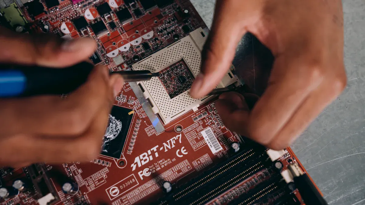
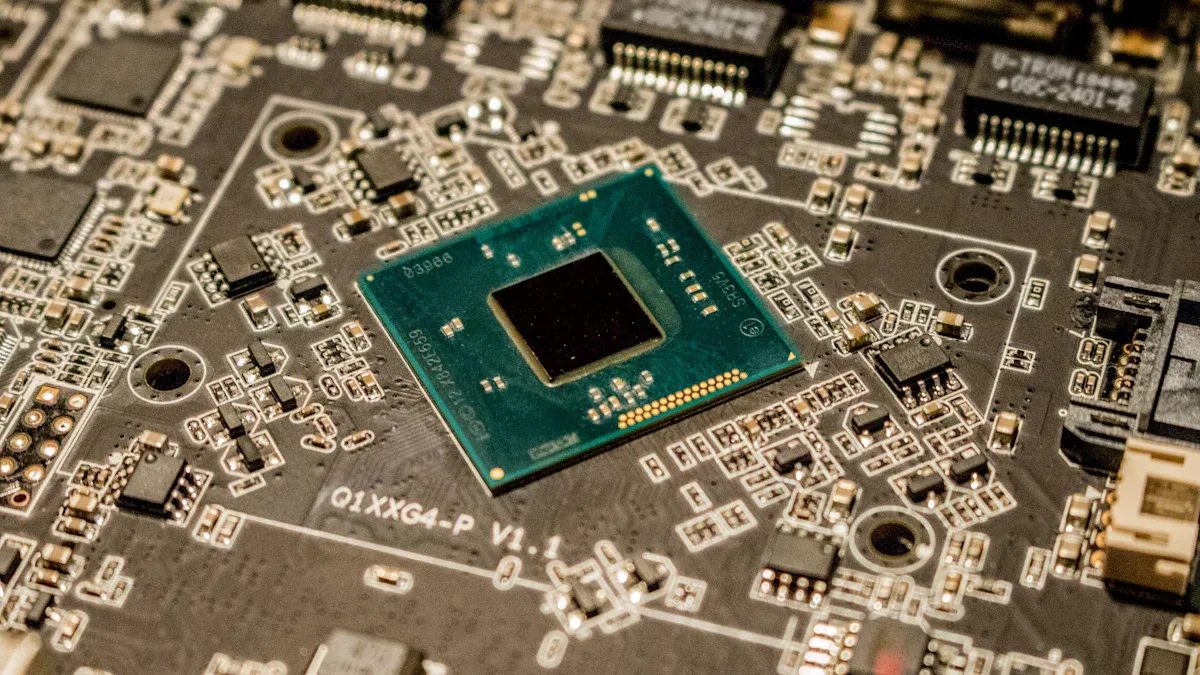
Avoiding Common Mistakes in Component Placement
Problems with Component Placement and Orientation
Placing parts correctly is very important for SMT PCBs. Mistakes in placement can cause big problems for how they work.
Misplaced parts can cause electrical shorts and mess up signals.
Wrong placement can make parts too hot and damage them.
Assembly errors often happen when schematics and Gerber files don’t match.
Finding placement mistakes early is very important. Looking at the board can help spot visible issues like misaligned parts. Machines like AOI use technology to find placement and direction errors quickly. Electrical tests check if the PCB works and find any problems.
Method | What It Does |
|---|---|
Visual Inspection | Finds visible problems like crooked parts or solder mistakes. |
Automated Optical Inspection | Uses machines to spot placement and direction mistakes. |
Electrical Testing | Checks if the PCB works and finds any issues. |
Fixing these mistakes early saves money and makes your PCB more reliable.
Best Practices for Accurate Component Placement
Placing parts the right way helps the PCB last longer and work better. Following these tips can help avoid mistakes and improve performance.
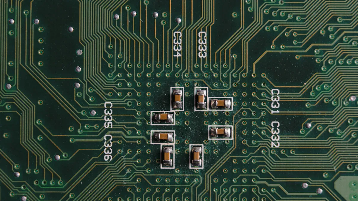
Put parts in smart spots to help signals move and manage heat.
Add decoupling capacitors near power pins to keep voltage steady.
Keep analog and digital circuits apart to stop signal problems.
Leave enough space between parts to prevent overheating and make routing easier.
Don’t place parts too close to the edges to protect them during production.
Shorter traces make signals stronger and reduce noise. Good placement lowers electromagnetic interference (EMI), making signals clearer. Enough space helps cool the board and stops overheating. Using verified CAD models and following library rules can make designs more reliable and save time.
Best Practice | Why It Helps |
|---|---|
Proper Component Placement | |
Use of Decoupling Capacitors | Keeps voltage steady and reduces noise near fast parts. |
Avoiding Signal Interference | Separates analog and digital circuits to keep signals clear. |
Adequate Component Spacing | Stops overheating and makes routing easier, improving reliability. |
Maintaining Edge Clearance | Protects parts from damage during production. |
By using these tips, you can avoid placement problems and make sure your PCB works well with today’s technology.
PCB Layout and Routing for Surface Mount Technology
Common Layout and Routing Mistakes
Mistakes in PCB layout can cause big problems. These errors affect how well the PCB works and how easy it is to make. Knowing these common mistakes can help avoid them:
Component Placement Errors: Parts placed wrong can stop current flow and cause failures.
Routing Problems: Missing connections or bad trace sizes can cause overheating or broken circuits.
Grounding Issues: Weak grounding adds noise and makes signals unclear.
Crosstalk: Traces too close together can mess up signals with interference.
Impedance Mismatches: Wrong impedance can distort signals and mess up timing.
Ignoring Design Rules: Breaking design rules can make the PCB hard to produce.
Mistake Type | What Happens |
|---|---|
Component Placement | Wrong placement can make parts fail. |
Routing Errors | Missing or bad connections can cause overheating or broken circuits. |
Power Distribution Errors | Thin traces for power can make the supply unstable. |
Grounding Issues | Weak grounding adds noise and ruins signal quality. |
EMI Problems | Fast traces near sensitive parts can cause interference. |
Solutions for Optimized PCB Layout and Routing
Good PCB layout and routing can fix these problems. Following smart design tips makes the PCB work better and easier to produce:
Maintain Consistent Trace Widths: Use the same trace size to handle current and stop overheating.
Control Impedance: Design traces to match impedance for clear, fast signals.
Place Decoupling Capacitors Strategically: Put capacitors near power pins to keep voltage steady and reduce noise.
Ensure Proper Grounding: Use a solid return path to lower noise and keep signals strong.
Avoid Sharp Bends: Make smooth curves in traces to stop signal problems.
Follow DFM Guidelines: Stick to design rules to avoid production mistakes.
Methodology | Why It Helps |
|---|---|
Controlled Impedance | Keeps signals clear and timing accurate. |
Decoupling Capacitors | Steadies voltage and lowers noise in fast circuits. |
Proper Grounding | Reduces noise and keeps signals strong. |
Smooth Trace Routing | Stops signal problems and improves performance. |
DFM Compliance | Makes sure the PCB can be made without errors. |
Using these tips can solve layout problems and improve PCB performance. This makes the PCB reliable and easier to manufacture.
Material Selection for SMT PCB Design
Problems with Choosing PCB Materials
Picking the right materials for SMT can be tricky. Wrong choices can hurt how well your PCB works and lasts. Different material properties can make drilling and plating harder. Substrates with varying dielectric constants can mess up signal flow, causing distortion.
When layers expand differently with heat, it creates stress. This stress can lead to layers peeling apart during temperature changes. The resin's glass transition point shows how much heat the material can handle. If it gets too hot, the PCB might fail. Changes in materials can also affect how heat spreads, needing changes in power plane design to manage heat better.
The table below lists common problems with PCB materials:
Problem | What Happens |
|---|---|
Fabrication Issues | Material differences make drilling and plating harder. |
Electrical Problems | Different substrates can mess up signal flow and impedance. |
Heat Expansion Differences | Layers expanding differently can cause stress and peeling. |
Heat Limit of Resin | Too much heat can damage the PCB during soldering. |
Heat Management | Material changes can affect heat spreading, needing design adjustments. |
Knowing these problems helps you pick better materials for SMT.
Tips for Picking the Right Materials
Choosing good materials makes sure your PCB works well with SMT. Start with high-quality materials. These are key for making strong and reliable PCBs. Think about how well they perform and how long they last.
Pick substrates that fit your product’s needs. Rigid, flexible, or metal-based options have different benefits, especially for handling heat in lead-free processes. Copper foil should be thick and good quality for better conductivity. For multilayer PCBs, use the right thickness to keep performance steady.
Inks and resins should stick well and handle high soldering heat. Use trusted brands for consistent results. Other materials, like those for drilling and bonding, also affect PCB quality. Always check materials when they arrive and manage their shelf life properly.
The table below shows what to consider when picking materials:
Material Type | What to Look For |
|---|---|
High-Quality Materials | Strong base for reliable PCBs; think about performance and durability. |
Substrate Choice | Match to product needs (rigid, flexible, metal-based) and heat handling for lead-free processes. |
Copper Foil | Thick, high-quality foil improves conductivity; use the right thickness for each layer. |
Inks and Resins | Must stick well and handle soldering heat; use trusted brands. |
Other Materials | Includes items for drilling and bonding; these affect overall PCB quality. |
Material Inspection | Check all materials before use; manage shelf life carefully. |
By following these tips, you can choose materials that make your SMT PCB design work better and last longer.
Manufacturing Tolerances and Design Rules in SMT
Problems Related to Tolerances and Design Rules
Manufacturing tolerances and design rules are very important for SMT PCB production. Ignoring them can cause problems that hurt how well your PCB works.
Setting correct tolerances helps manufacturers check if your design is possible. Without this, issues like shorts or misaligned parts can happen. Components must also meet size and shape rules for proper assembly. Leads that aren’t flat can make weak solder joints, which lowers PCB quality.
Common problems include tight tolerances causing more scrap and higher costs. Studies show fixing stencil and placement data reduces defects. For example, Motorola cut solder paste errors by 43%, and ScanCAD lowered tombstoning by over 60%.
Study | What Was Done | Result |
|---|---|---|
Motorola Study | Changed stencil data to match PCB | 43% fewer solder paste defects |
ScanCAD Study | Adjusted stencil and placement data | Over 60% less tombstoning |
Solutions to Ensure Compliance with SMT Requirements
To fix these problems, follow DFM rules and SMT design guidelines. Accurate part placement improves production and lowers mistakes. Using verified CAD models and following DFM rules helps avoid errors.
Set tolerances that match manufacturing standards. Keep enough space between parts to stop shorts. Use flat leads for strong solder joints. Include files like netlists and follow industry rules to meet requirements.
Tools like thermal modeling and AOI can check designs before production. These tools find problems early, saving time and money. Picking good materials and keeping trace widths consistent also helps.
Technical documents explain why precision matters in PCB design. Guides on part placement and tolerances show how following rules improves production.
Source | Evidence Type | Summary |
|---|---|---|
Design Guidelines | Talks about accurate placement and DFM rules. | |
Essential Documentation for Manufacturing Bare PCBs and FPCs | Compliance Documentation | Lists needed documents for manufacturing standards. |
Tolerance Specifications | Explains why tolerances matter in PCB design. |
By using these solutions, you can make sure your SMT PCB design meets manufacturing rules. This reduces mistakes and makes production better.
LT CIRCUIT’s Expertise in Solving PCB Design Challenges
Smart Solutions for Signal Integrity and Heat Control
Fixing signal and heat problems needs smart ideas. LT CIRCUIT uses advanced tools to make PCBs work better and last longer.
Linear RF Technology keeps signals clear and saves power.
Broadband Amplifiers boost efficiency while keeping signals steady.
Variable Gain Technologies adjust signals for modern needs.
Harmonic Management removes bad frequencies to keep signals clean.
These tools solve common PCB issues. For example, notch filters cut signal noise, and pre-distortion fixes signal errors for better communication.
Feature | What It Does | Why It Matters |
|---|---|---|
Linear RF Amplifiers | Save power while keeping signals strong. | Stops distortion and keeps communication clear. |
Variable Gain RF Amplifiers | Adjust signal strength for different needs. | Improves speed and lowers delays. |
Harmonic Suppression Techniques | Remove unwanted frequencies from signals. | Makes signals cleaner and reduces errors. |
Distortion Mitigation Techniques | Fix signal errors with pre-distortion methods. | Improves communication quality and range. |
These ideas help your PCB design meet today’s technology needs and stay reliable.
High-Tech PCB Products for Surface Mount Technology
LT CIRCUIT makes advanced PCBs for surface mount technology. These products use AI and automation to work faster and more accurately. Automation also lowers mistakes and saves money.
Surface mount PCBs are used in many industries like phones, cars, and medical devices. Small devices in telecom use SMT to send data faster. Medical tools need precise PCBs to meet safety rules.
The PCB market was worth $70 billion in 2020. It’s expected to grow 3.4% yearly until 2028. Demand for electronic parts may rise 10% by 2030. LT CIRCUIT’s products match these trends with high-tech designs for modern uses.
Statistic | Value |
|---|---|
PCB market size (2020) | $70 billion |
Growth rate (2021-2028) | 3.4% |
Electronic parts demand growth (2020-2030) | 10% |
Choosing LT CIRCUIT gives you access to smart products that fit the future of surface mount technology.
Fixing common PCB design problems for SMT helps make better products. Smart design steps, like improving solder paste use and solving heat issues, make PCBs more reliable. Using LT CIRCUIT’s advanced SMT tools can lower mistakes and boost success.
Statistic Type | What It Shows |
|---|---|
Shows how often PCBs are made correctly | |
Key Parameter Averages | Includes size, shape, and alignment details |
Process Consistency | Checks how steady the process is |
Smart design reduces mistakes and improves efficiency, helping your products meet today’s tech needs.
FAQ
How can you stop soldering problems in SMT PCB design?
Print solder paste carefully and use the right heat settings. Pick good finishes like ENIG to make strong solder joints and avoid mistakes.
What helps improve signal quality in fast PCB designs?
Use materials that lose less signal and plan trace paths well. Add decoupling capacitors to cut noise and make signals clearer.
Why is controlling heat important in SMT PCB design?
Too much heat can break parts and weaken solder. Use heat vias, sinks, and testing tools to handle heat better.
See Also
Key Considerations When Designing PCB Circuit Boards
Essential Skills for Multi-Layer PCB Layout Mastery
Crucial Guidelines for High Current Heavy Copper PCB Design
Utilizing Horizontal Copper Sinking Technology in PCB Manufacturing
Challenges in Manufacturing and Prototyping Multi-Layer Circuit Boards