How to Master Fine Line Control in the PCB Etching Process

Mastering fine line control in the pcb etching process lets you make clear pcb etching results. You must pay attention to accuracy with fine lines and spaces. Manufacturers deal with problems like small trace widths, signal interference, and overheating. You can solve these by checking fabrication limits, keeping good spacing, and using trace width calculators. These steps help you make circuit boards that work well and last long.
Key Takeaways
Getting good at fine line control in PCB etching helps make circuit boards clear and dependable.
Pick the right copper thickness to make traces more accurate and have fewer problems.
Try using advanced methods like semi-additive processes to control fine lines better.
Check your etching process often to find problems early and keep quality high.
Work with your manufacturer to make sure your design fits what they can build.
Why Fine Line Control Matters
High-Density PCB Demands
Devices are getting smaller and more powerful. You need to fit more parts and connections on each board. The pcb etching process must make fine lines and spaces for these tight layouts. High-resolution pcb etching helps you get thin traces and small pads. These are important for hdi pcbs. If you do not control etching well, you can get rough edges or uneven lines. These problems can cause electrical failures and make boards less reliable.
Tip: Using advanced methods like laser drilling helps you make exact via sizes. This improves both electrical and mechanical strength.
Industry rules set the smallest trace widths and spacing for boards. You must follow these rules to stop short circuits or bad etching. The table below shows common values:
Type of PCB | Minimum Trace Width | Minimum Trace Spacing |
|---|---|---|
Standard PCBs | 5-6 mils | 4-6 mils |
Advanced PCBs | 3-4 mils | 3-4 mils |
HDI Designs | As small as 3 mils | Down to 3 mils |
High-resolution pcb etching lets you meet these strict limits. Always check with your manufacturer before you finish your design.
Impact on Circuit Performance
Fine lines and spaces change how circuits work. Impedance control keeps signals strong in modern electronics. You need even transmission lines with controlled impedances to stop signal distortion. Bad impedance can cause crosstalk and electromagnetic interference. In fast interfaces, small mismatches can cause bit errors or reliability problems.
Bad impedance control raises error rates and electromagnetic emissions.
Good signal integrity comes from steady design rules and careful pcb etching process.
Faster signal rise times make distortion worse if you do not control line impedances.
You make circuits work better by mastering fine line control. High-density interconnect boards depend on these steps to give reliable results.
Key Factors in the PCB Etching Process
Copper Thickness Selection
Picking the right copper thickness is important for fine lines. Thin copper makes it easier to create narrow traces. It also helps with tight spacing. This choice improves etching accuracy. It helps you get high-resolution pcb etching for advanced designs. Thin copper can be sensitive to small changes during etching. Thick copper needs special tools to keep etching even and stop defects.
The table below shows good values for fine-line pcbs:
Feature | Measurement |
|---|---|
Copper Thickness | 12 micrometers (μm) |
Minimum Trace Width | 50 micrometers (2 mils) |
Minimum Trace Spacing | 50 micrometers (2 mils) |
Standard Trace Width | 75 micrometers (3 mils) |
Choosing the right copper thickness helps you get accurate trace width. It also lowers the risk of over-etching. Always check with your manufacturer to make sure their limits fit your design before you finish your layout.
Photoresist and Imaging
You need good photoresist and careful imaging for fine lines. The photoresist layer protects copper during etching. Uniform thickness and strong sticking are important for high-resolution pcb etching. Dry film, liquid resist, and ED resist each have their own benefits for fine-line work.
Parameter | Dry Film | Liquid Resist | ED Resist |
|---|---|---|---|
Thickness Range | 0.8-2.0 mil (20-50µm) | 0.5-50µm (adjustable) | 5-15µm |
Resolution | 30µm lines/spaces | 20-50µm lines/spaces | 15-25µm lines/spaces |
Best Application | General PCB production | Uneven surfaces | HDI, fine-line multilayer |
Cost | Medium | Low-Medium | High |
Process Complexity | Low | Medium | High |
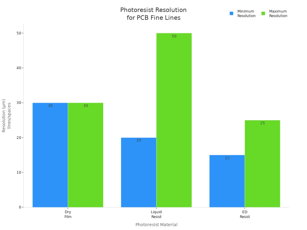
Follow best practices for photoresist to stop defects:
Clean copper well before putting on resist.
Use the right method for your production size.
Control developer strength and temperature.
Keep photoresist in a cool, dry place.
Laser Direct Imaging (LDI) gives the highest resolution. It can go down to 1 mil or less. This technology lowers alignment mistakes. It helps you get tighter tolerances for hdi pcbs.
Etching Chemistry and Parameters
You control fine lines and spaces by managing etching chemistry and process steps. The main factors are temperature, time, agitation rate, and etchant strength. Each one changes how copper dissolves and keeps the trace shape.
Temperature: Most etching runs at 40–50°C. Higher heat speeds up etching but can cause over-etching.
Time: Etching time decides how much copper is removed. Too little time leaves thin films. Too much time eats away trace edges.
Agitation Rate: Good agitation keeps fresh etchant touching copper. Bad agitation gives uneven results.
Etchant Concentration: Weak solutions cause patchy etching. Strong solutions can attack protected areas.
Timer-controlled etching systems help you keep tight control. These systems let you set exact times for each step. This improves consistency and accuracy. You can get line and space sizes down to 2 mil with these methods.
Design Alignment with Fabrication Limits
You must match your design to what your fabrication house can do. Each manufacturer has limits for minimum trace width and spacing. If you use values below their limits, you risk defects like over-etching or under-etching. For standard boards, trace width and spacing are usually 5 to 8 mils. Advanced facilities can go below 3 mils with special tools.
Type of PCB | Minimum Trace Width (mils) |
|---|---|
Standard PCBs | 5-6 |
Advanced PCBs | 3-4 |
Specialty | Below 3 |
Manufacturing tolerances matter too. Standard processes allow ±10-20% change in trace width. High-precision processes can get ±5% or better. Always work with your manufacturer and follow their guidelines. This makes sure your fine-line pcbs meet both electrical and production needs.
Tip: Work with your fabrication partner to adjust your design for their limits. This step helps you avoid costly mistakes and ensures reliable results.
Advanced Etching Techniques
Semi-Additive Process (SAP)
You can get better control of fine lines with the semi-additive process. SAP begins with a very thin copper layer. A photoresist is put on top. Copper is added only where you want the traces. This method builds the circuit instead of taking away lots of copper. You get cleaner and straighter trace shapes. The features can be much smaller. The table below shows how SAP and traditional etching are different:
Feature | mSAP | Traditional Etching |
|---|---|---|
Starting Material | Thin copper | Thick copper |
Process Type | Selective plating | Etching excess copper |
Trace Profile | Vertical, precise | Prone to undercut |
Line Width Capability | 10–20 μm (advanced) | Wider traces |
Best Use | High-density designs | Standard designs |
SAP lets you make traces as thin as 15 microns. This process helps with high routing density and advanced PCB designs.
Plasma and Laser Methods
Plasma and laser methods help you make very tiny features. Plasma etching uses special gases in a vacuum to remove copper or dielectric material. This way does not use chemicals. It makes less waste and gives clean edges. Laser etching uses strong lasers to cut copper very accurately. You do not need photomasks, so you can change designs fast. Laser etching is good for microvias and high-frequency boards that need very small details.
Benefits of Plasma and Laser Etching:
Plasma etching makes very little chemical waste and gives great control over how deep you etch.
Laser etching is good for making new designs quickly and works well for tricky, small projects.
Both ways need special machines to work best.
Note: Plasma and laser etching let you make features smaller than 25 micrometers. This is important for advanced electronics.
Timer-Controlled Etching Systems
Timer-controlled etching systems help you be more exact and steady. These systems let you pick the exact time for each step. Good control makes sure copper is removed just right. This lowers mistakes and keeps trace widths the same everywhere. Timer-controlled systems are important for making lots of boards where you need the same results every time.
Quality Control and Process Optimization
In-Process Monitoring
You have to check fine lines and spaces at every step. This helps you find problems early and keep things the same each time. You should use electrical tests, lab checks, and look at the boards closely to see if they are good. The table below lists ways to check quality:
Description | |
|---|---|
Electrical Test | Uses Flying Probe Test and Fixture Test to check if the PCB works right. |
Physical Lab Testing | Looks at the board with special microscopes and X-rays for a close check. |
Quality Inspection Before Shipment | Follows ISO9001:2015 and IPC rules with strong electrical and visual checks. |
Quality Control Process | Uses new tools to keep making the process better and safer. |
Tip: Checking often helps you keep trace widths the same and makes sure signals stay strong in your circuits.
Defect Detection
You need to find and fix problems fast so your boards work well. Some common problems in fine line PCB etching are pinholes, bridging, and lines that are not the same width. The table below shows these problems and how to spot them:
Defect Type | Description | Detection Method |
|---|---|---|
Pinholes | Tiny holes in copper lines from dirt before photoresist. | Look with a microscope |
Bridging | Extra copper between lines from not enough etching. | Use an automatic optical check |
Line Width Variation | Lines that are too thick or thin from heat or mixing problems. | Cut and look at a cross-section |
To fix these problems, you can:
Try MSAP or mSAP to stop burrs and bridging.
Get better exposure tools for good alignment and fewer mistakes.
Change etching time and chemicals to get the right results.
Continuous Improvement
You make your process better by checking results and changing what you do. New control systems let you change etching as you work. Better photoresist gives sharper lines and sticks better. Improved ways to add chemicals help you remove copper only where you want. The table below shows how these steps help you control fine lines:
Evidence Description | Contribution to Fine Line Control |
|---|---|
Advanced process control systems | Makes sure material is removed evenly and patterns are clear. |
Optimized photoresist materials | Gives sharper edges and stands up to etching better. |
Improved chemical composition and delivery | Removes copper only where needed for neat circuit lines. |
Note: Always working to improve keeps your process steady and helps you make good boards every time.
You can get better at fine line control in PCB etching by doing some important things.
Keep the right temperature and mix the etchant well.
Make sure copper is ready so photoresist sticks strong.
Stop dirt and dust by keeping everything very clean.
Use new imaging and semi-additive ways for closer control.
Checking your process often and looking for mistakes helps you make more good boards. Using high standards and new methods lets you build smaller, faster, and stronger PCBs that work well.
FAQ
What is the smallest trace width you can achieve with modern PCB etching?
Advanced etching methods like SAP or laser etching can make traces as small as 2–3 mils. You should ask your manufacturer what sizes they can do.
How do you prevent over-etching fine lines?
You need to watch etching time and temperature carefully. Timer-controlled systems help you keep things steady. Clean copper and good photoresist also stop over-etching.
Why does copper thickness matter for fine line PCBs?
Thin copper helps you make narrow traces more easily. You get better accuracy and fewer problems with undercutting. Always pick copper thickness based on your design and what your manufacturer can handle.
Can you use standard PCB design rules for fine line etching?
No, standard rules do not work for fine lines. Fine line designs need tighter controls and special steps. Always match your design to your fabrication house’s fine line abilities.
What defects should you watch for in fine line PCB etching?
Pinholes
Bridging
Line width variation
You should check boards with microscopes and automatic optical inspection to find these problems early.
See Also
Tips For Excelling In PCB Quality Control Processes
A Guide To Immersion Tin Finishes In PCB Design
How Vacuum Two-Fluid Etching Enhances PCB Precision
