PCB Fabrication Manufacturer Capabilities and What LT CIRCUIT Offers for Complex Designs
Advanced PCB Fabrication plays a vital role in delivering reliable, high-performance electronic products. Top manufacturers use detailed documentation like Gerber and BOM files to ensure each board meets strict design specifications. LT CIRCUIT leads the industry by combining innovative technology with strong quality control. Inadequate manufacturing can result in defects that early electrical and functional testing might reveal.
Key Takeaways
Strong design support and advanced materials help create reliable, high-performance PCBs for complex projects.
LT CIRCUIT uses cutting-edge technology and strict quality control to deliver precise, custom PCB solutions quickly and consistently.
Thorough testing and international certifications ensure every PCB meets high standards for safety and durability.
PCB Fabrication Capabilities
Design Support
Strong design support forms the foundation of successful PCB Fabrication for complex projects. Leading manufacturers provide engineering expertise at every stage, from initial concept to final production. They help customers select the right stack-up, optimize layouts, and ensure manufacturability. The electronics industry has seen rapid growth, with the PCB market expected to reach over $100 billion by 2032. This expansion drives the need for advanced engineering support, especially as devices become smaller and more powerful. Companies now require help with high-density layouts, signal integrity, and compliance with industry standards. Top manufacturers offer services like Design for Manufacturability (DFM) checks, rapid quoting, and 24/7 technical support. These features reduce errors, speed up development, and help customers bring products to market faster.
Material Options
Material selection plays a critical role in PCB Fabrication, especially for high-speed or high-power applications. Manufacturers offer a wide range of materials, each with unique electrical, thermal, and mechanical properties. For example, FR4 is popular for its durability and cost-effectiveness, while high-frequency laminates like Rogers or Taconic maintain signal integrity at GHz speeds. Metal core PCBs use aluminum or copper bases to improve heat dissipation, which is essential for LED lighting and power electronics. Rigid-flex materials combine flexibility and strength, making them ideal for aerospace and medical devices. Key properties such as dielectric constant, thermal conductivity, and glass transition temperature influence performance and reliability. Selecting the right material ensures the board can handle demanding environments and complex designs.
Tip: Choosing the correct material can improve heat dissipation by up to 55 times and reduce signal loss in high-frequency circuits.
Advanced Techniques
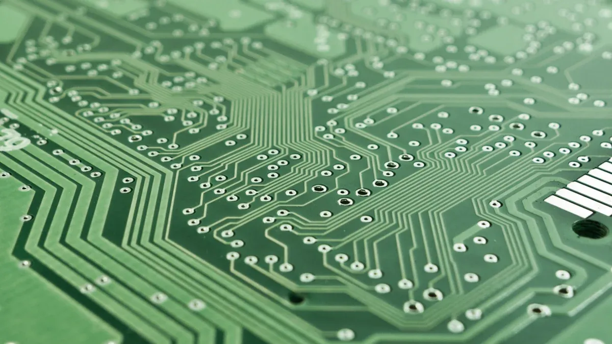
Modern PCB Fabrication uses advanced techniques to meet the needs of high-density and multi-layer designs. Manufacturers now produce boards with more than 20 layers, using technologies like laser direct imaging and microvia drilling. These methods allow for ultra-fine features, such as 15μm line spacing and 50μm microvias, which are essential for 5G and high-speed data applications. Innovations like stepped copper coin insertion improve thermal management, while embedded components save space and boost performance. Automated processes and smart manufacturing tools help maintain precision and consistency, even as designs become more complex. These capabilities set top manufacturers apart and enable them to serve industries like automotive, telecommunications, and aerospace.
Multi-layer lamination supports thin, high-density substrates.
Laser cutting enables complex shapes and precise impedance control.
Embedded components and advanced via technologies address miniaturization challenges.
Quality Standards
Quality standards ensure that every PCB meets strict requirements for safety, reliability, and performance. Leading manufacturers follow international certifications such as ISO 9001, IATF 16949, and UL. They use a range of inspection and testing methods to catch defects early and maintain high standards. Automated Optical Inspection (AOI), X-ray inspection, and In-Circuit Testing (ICT) detect both visible and hidden issues. Functional and environmental stress tests confirm that boards work under real-world conditions. Manufacturers also track components and materials for traceability and store them in controlled environments to prevent damage.
Quality Control Method | Description | Impact on High Standards |
|---|---|---|
Automated Optical Inspection (AOI) | High-resolution cameras detect surface defects | Early defect detection, improved yield |
X-Ray Inspection | Non-destructive testing of internal structures | Finds hidden defects, ensures reliability |
In-Circuit Testing (ICT) | Electrical probing for circuit integrity | Verifies correct assembly and performance |
Functional Testing | Simulates operational environment | Confirms boards meet functional requirements |
Environmental Stress Testing | Exposes boards to heat, humidity, vibration | Assesses durability in harsh conditions |
Compliance with ISO, IPC, UL, and other standards | Guarantees consistent quality and safety |
Prototyping
Prototyping is a key step in PCB Fabrication, especially for complex designs. Quick-turn prototyping allows engineers to test ideas, identify flaws, and make improvements before full-scale production. This process reduces costly errors and shortens development cycles by up to 50%. Comprehensive testing during prototyping includes functional, environmental, and compliance checks. Automated design rule checks catch mistakes early, improving prototype success rates. Reliable manufacturers offer fast lead times, sometimes delivering prototypes in as little as 8 hours. These services help customers bring products to market quickly and with greater confidence.
Early risk mitigation lowers the chance of expensive mistakes.
Rapid iterations speed up time-to-market.
Automated testing increases reliability and stakeholder trust.
LT CIRCUIT Advantages
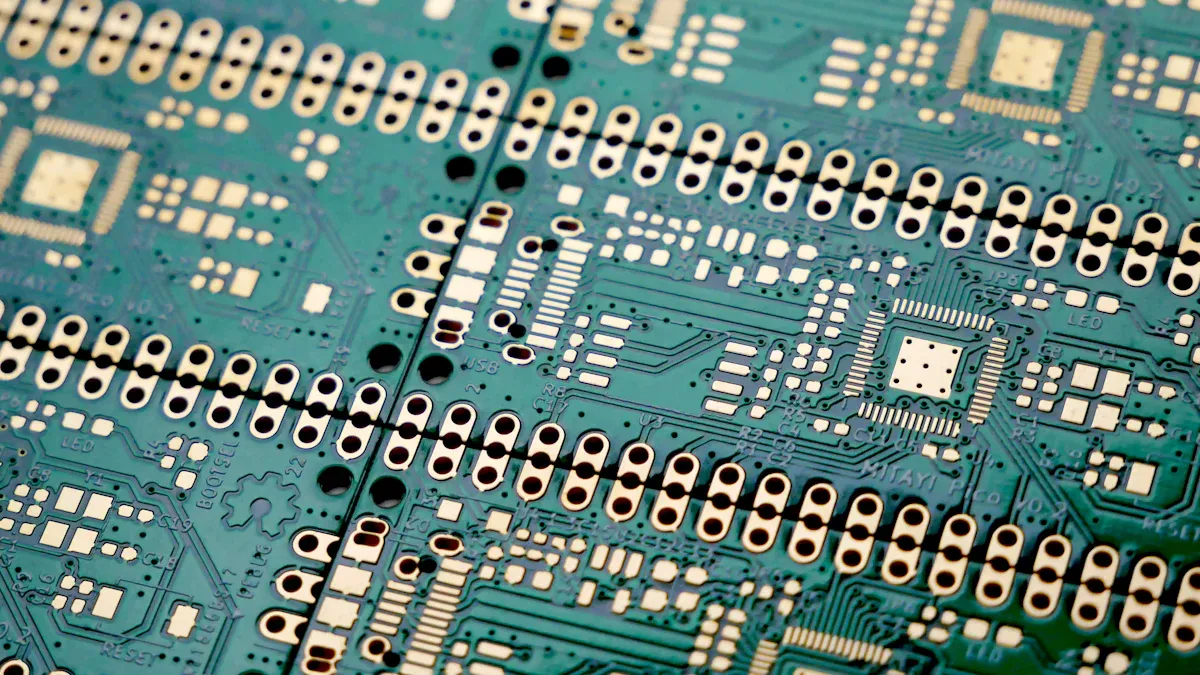
LT CIRCUIT PCB Fabrication
LT CIRCUIT stands out in PCB Fabrication by offering a wide range of advanced solutions. The company produces high-density interconnect (HDI) boards, multilayer PCBs, and any-layer HDI products. These options support complex designs for industries like telecommunications, aerospace, and medical devices. LT CIRCUIT uses cutting-edge materials and processes, such as laser direct imaging and microvia drilling, to achieve fine line widths and tight spacing. The company can manufacture boards with up to 12 layers and a maximum thickness of 8.0 mm. Strict quality control, including operator self-inspection and QA sampling, ensures consistent results.
Parameter | Specification |
|---|---|
Minimum line width/spacing | 3 mil / 3 mil (copper thickness 0.5 OZ) |
Maximum board thickness | Up to 8.0 mm (single/double and multilayer) |
Maximum number of layers | 12 layers |
Certifications | UL, CE, ISO-9001, SGS lead-free |
These capabilities allow LT CIRCUIT to deliver reliable PCB Fabrication for both high-volume and specialized projects.
Engineering Expertise
LT CIRCUIT employs a team of experienced engineers who guide customers through every stage of PCB Fabrication. The engineering team helps with stack-up design, material selection, and layout optimization. They use advanced tools like Statistical Process Control (SPC), AI-driven predictive models, and Digital Twin Models to monitor and improve production. Automated Optical Inspection (AOI) and X-ray inspection tools detect and reduce defects. These methods have helped clients achieve impressive results, such as a 99.8% first-pass yield rate for an aerospace company and a 40% faster product launch for a medical device firm.
Example Company | Improvement Focus | Outcome Metric |
|---|---|---|
Medical Device Firm | Faster product launch | 40% faster launch time |
Aerospace Company | First-pass yield rate | 99.8% yield rate |
The engineering team’s expertise ensures that each project meets strict industry standards and customer requirements.
Custom Solutions
LT CIRCUIT offers custom solutions tailored to unique project needs. Customers can choose from a variety of surface finishes, such as ENIG, HASL, and immersion silver. The company provides different solder mask colors and supports embedded components for miniaturized designs. Testing services include flying probe tests and E-tests, which verify board performance before delivery. LT CIRCUIT’s flexible approach allows it to serve a diverse customer base, from consumer electronics to industrial equipment manufacturers.
Note: LT CIRCUIT’s customization options help customers solve design challenges and bring innovative products to market faster.
Quality Assurance
Quality assurance remains a top priority at LT CIRCUIT. The company follows international standards, including ISO 9001, UL, and CE certifications. Advanced inspection tools, such as AOI and X-ray, help reduce defects by up to 40% in high-volume production. The use of SPC and predictive analytics ensures that each board meets strict quality requirements. Environmental and functional testing confirm that products perform reliably in real-world conditions. These practices support high first-pass yields and low defect rates, making LT CIRCUIT a trusted partner for demanding applications.
Industry Recognition
LT CIRCUIT has earned recognition for its innovation and reliability in PCB Fabrication. The company serves leading brands in consumer electronics, telecommunications, and industrial sectors. Its achievements include developing advanced PCB technologies and maintaining high production standards. LT CIRCUIT’s manufacturing process uses smart-cut wafer substrate fabrication and optimized dry etching, which enable scalable and cost-effective production. The company’s performance metrics, such as low intrinsic optical loss and superior propagation loss, set it apart from competitors.
Metric / Feature | LT CIRCUIT Performance / Advantage | Industry Benchmark |
|---|---|---|
Intrinsic optical loss rate | 26.8–82 MHz (depending on wafer treatment) | ~50.8 MHz or higher |
Propagation loss | As low as 5.6 dB/m | 27 dB/m |
Lithography and etching | Optimized dry etching, steep angles (~70°) | Varies, often less precise |
Manufacturing process | Smart-cut, scalable, cost-effective | Less scalable, higher cost |
Substrate availability | Low-cost, widely used LiTaO3 substrates | Less available, higher cost |
LT CIRCUIT’s combination of advanced technology, strict quality control, and customer-focused solutions makes it a leader in the PCB Fabrication industry.
Advanced manufacturing capabilities ensure complex designs meet strict reliability standards. Rigorous internal testing and third-party certifications confirm high performance. LT CIRCUIT delivers proven expertise and trusted quality for demanding projects. Readers can explore LT CIRCUIT’s solutions or contact the team for expert consultation.
FAQ
What industries benefit most from LT CIRCUIT’s PCB solutions?
LT CIRCUIT serves telecommunications, aerospace, medical, consumer electronics, and industrial sectors. These industries need advanced, reliable, and high-density PCB designs for their products.
How does LT CIRCUIT ensure PCB quality?
LT CIRCUIT uses AOI, X-ray inspection, and strict quality control. The team follows ISO 9001 and UL standards. Every board passes multiple tests before delivery.
Can LT CIRCUIT handle custom PCB requests?
Yes, LT CIRCUIT offers custom finishes, solder mask colors, and embedded components.
The engineering team supports unique layouts and special requirements for complex projects.
See Also
Challenges And Steps In Multi-Layer Circuit Board Prototyping
Step-By-Step Guide To Printed Circuit Board Production
Comprehensive Overview Of The PCB Fabrication Procedure
Role Of LDI And CCD Technology In PCB Manufacturing
Essential Questions To Discuss With PCB Makers Before Production