How PCBs Are Made A Detailed Fabrication Process
Making PCB fabrication requires careful steps to build strong circuit boards. This process is crucial for today’s advanced electronics. For example, car PCBs must handle temperatures ranging from -40°C to 85°C. This demonstrates the stringent standards involved in their production. LT CIRCUIT guarantees top quality in every step.
Key Takeaways
Planning a PCB layout well saves time and money. Use design software to make it accurate and fast.
Picking good materials is important for strong PCBs. Think about heat resistance and signal strength when choosing them.
Tests like electrical checks and looking for flaws are key. They make sure the PCB works right and follows rules.
Design and Preparation in PCB Fabrication
The design and preparation step is the start of making a PCB. It makes sure the board works as planned and meets all needs. This step includes making a layout, preparing files, and picking materials.
PCB Design and Layout
The first task is to design the PCB layout. Special software like Altium Designer or Eagle helps create a plan. This plan shows how parts and connections will fit on the board.
A good design avoids mistakes and saves time. For example, if most designs pass on the first try, it reduces costs. Faster design times also help you finish projects quickly and stay ahead.
Metric | What It Means | Why It Matters |
|---|---|---|
How many designs pass on the first try. | Fewer retries mean lower costs and better accuracy. | |
Design Cycle Time | Time from idea to final design approval. | Shorter times make the process smoother and faster. |
Defect Density | Number of mistakes in each PCB area. | Fewer mistakes mean better quality boards. |
Focusing on these points helps make designs better and more reliable.
Preparing Gerber Files for PCB Manufacturing
After designing, Gerber files are created. These files are like a map for making the PCB. They include details about copper layers, solder masks, and labels.
Gerber files follow strict rules to work with machines. Standards like IPC-A-610 ensure things like clean soldering. Following these rules means your PCB will meet high-quality standards. Audits by outside groups often check this for extra confidence.
Material Selection for PCB Manufacture
Picking the right materials is very important for making a good PCB. The base material, often FR4, gives the board strength and insulation. Copper layers carry electricity, and solder masks protect the board from damage.
Industry rules guide material choices. For example, IPC rules set limits and tests for durability. These rules help make strong PCBs that handle heat and stress well.
Things to think about when choosing materials:
Can it handle high heat?
Does it send signals well?
Is it strong enough for physical stress?
Choosing the best materials improves how long your PCB lasts and how well it works.
Tip: Talk to your manufacturer to make sure materials match your design and meet industry rules.
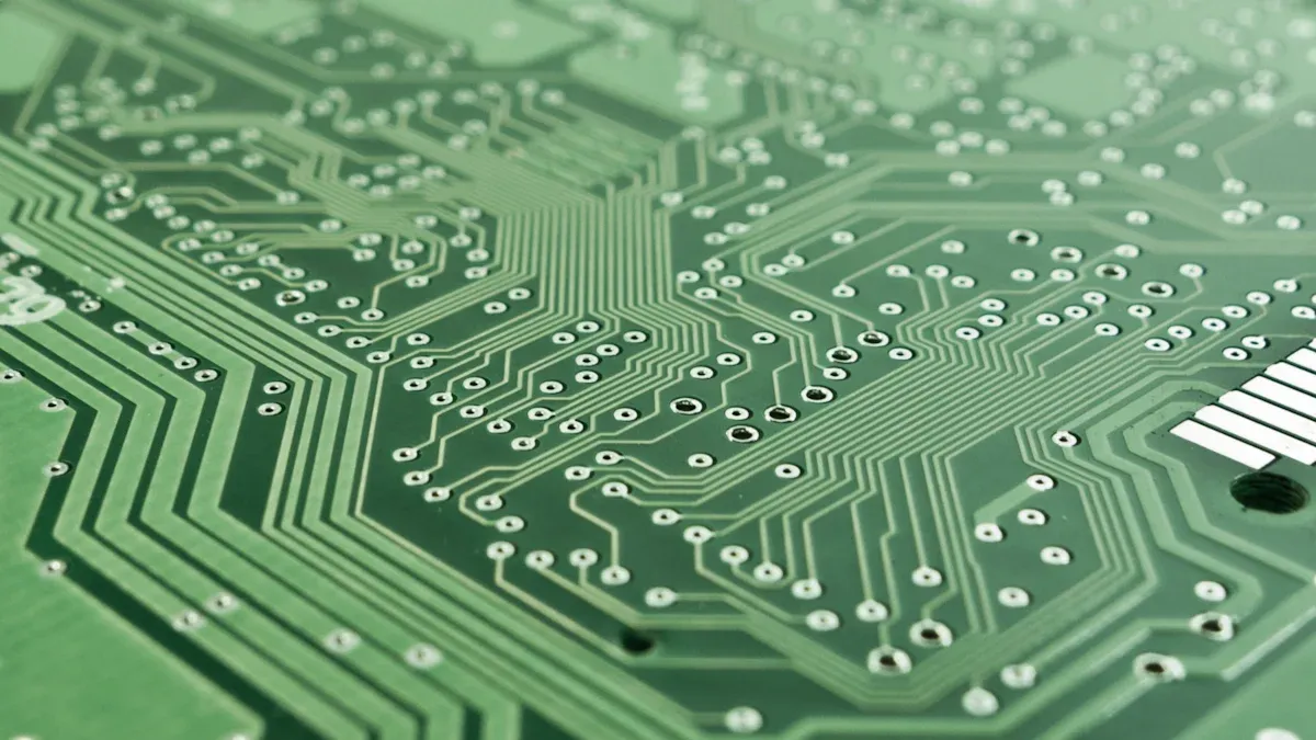
Inner Layer Processing in the PCB Manufacturing Process
Photoresist Application
The first step is adding photoresist to the copper. This material reacts to light and forms the circuit pattern. Manufacturers use special methods to spread it evenly. Purity and uniformity are very important. Tiny impurities can harm performance. Adhesion promoters must be even at a molecular level. This reduces pattern collapse by 40%. These steps help the photoresist stick well and work properly.
Metric | Description |
|---|---|
Purity Levels | Impurities over 0.1 parts per trillion (ppt) lower performance. |
Molecular Uniformity | Even adhesion promoters cut pattern collapse rates by 40%. |
Performance Characteristics | pH and ionic balance prevent swelling or erosion in sensitive resists. |
UV Exposure and Image Development
Next, UV light shines on the photoresist to create the circuit. The light hardens some areas, leaving others soft. A developer solution washes away the soft parts. This reveals the copper underneath. This step transfers the circuit design onto the board.
Etching the Copper Layers
Etching removes extra copper from the board. This leaves only the circuit pattern behind. Manufacturers control etching carefully to avoid mistakes. They also check copper thickness for consistency. These steps ensure the board matches the design.
Inner Layer Inspection
The last step is checking the inner layers for problems. Technicians look for shorts, gaps, or weak spots. They also measure conductor width and spacing for accuracy. Clean surfaces are very important too. The table below shows key checks during this step:
Stage of Process | Quality Measurements/Checks |
|---|---|
Base Material & Resist Quality Checks | Core material flaws, Copper roughness, Photoresist thickness, curing, and adhesion |
Post-exposure & Development Check | Image size, leftover material, Complete resist removal in circuits |
Etching Quality Inspection | Etch depth, Overcut or undercut checks, Copper thickness consistency |
Final Innerlayer Quality | Circuit spacing, Surface cleanliness, Conductor width, No shorts, gaps, or weak spots |
These steps make sure the inner layers are strong and meet standards.
Layer Lamination in PCB Fabrication
Aligning the Layers
This step makes sure all PCB layers line up. Each layer has detailed patterns that must match perfectly. Machines with optical systems help align layers accurately. These systems ensure copper paths and holes connect properly.
The alignment is kept within ± 75μm for precision. Tight control reduces errors and improves PCB reliability. Even small misalignments can break connections and cause problems. To prevent this, manufacturers check alignment several times. This step is key to making a strong and working circuit board.
Pressing and Bonding Layers Together
After aligning, the layers are pressed together. Heat and pressure join them into one solid piece. A special press applies even pressure across the stack. Heat melts the prepreg, a resin-coated fiberglass sheet, bonding the layers.
It’s important to avoid air bubbles or gaps between layers. These flaws can weaken the board and hurt its performance. Pressing also secures the copper paths, keeping them safe for later steps. Once cooled, the laminated board becomes strong and ready for use.
Tip: Good lamination helps your PCB handle tough electronic demands.
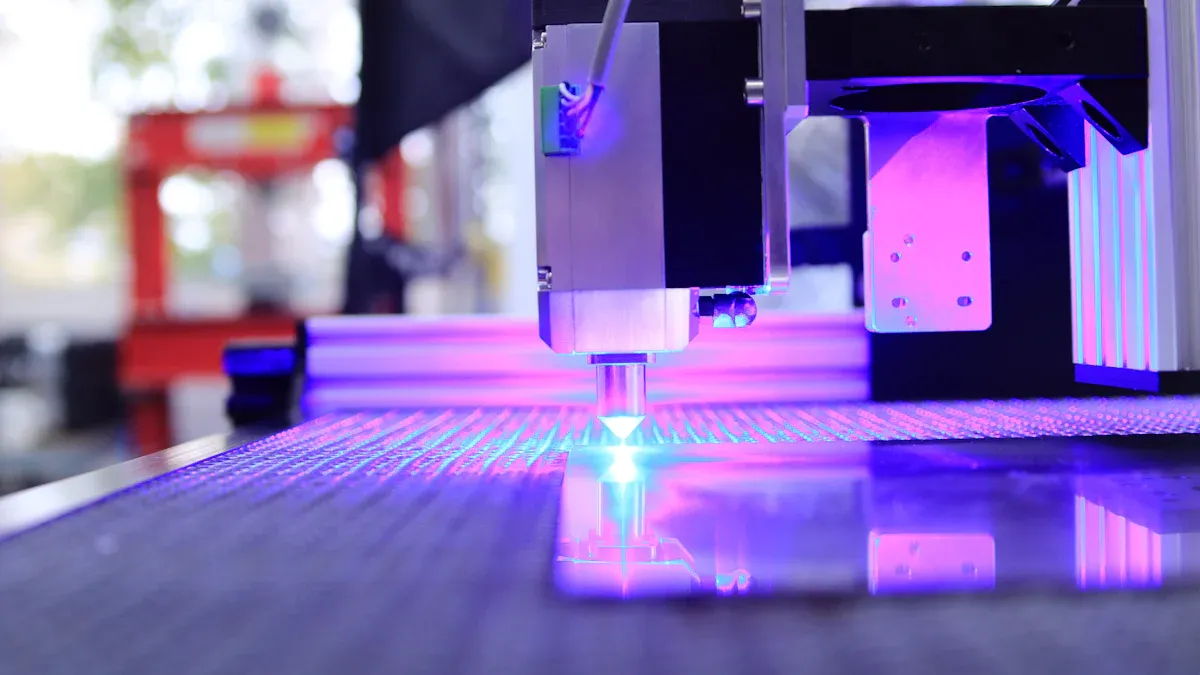
Drilling and Plating in PCB Manufacture
Drilling Holes for Vias and Components
Drilling is a very important step in making PCBs. Holes are made for vias and parts to connect layers. These holes let electricity move through the board. Machines with special drills make sure holes are precise. The drills work fast to cut cleanly without harming the board.
If holes are not round, problems can happen in advanced PCBs. Studies show 38% of tiny via issues come from bad hole shapes. To fix this, manufacturers use methods to make holes more round. They reduce shape errors from 8μm to 2.5μm in 6-layer boards. This improves signal flow and makes the PCB more reliable.
Copper Plating for Electrical Conductivity
Copper plating is needed to make paths for electricity. After drilling, copper is added to the holes to link layers. This process creates a surface that carries electricity well. It lowers resistance and helps signals move better. This is very important for high-speed circuits.
Modern copper plating methods make sure paths have low resistance. This helps signals stay strong, even in tough conditions. Whether your PCB is simple or complex, copper plating is key to its success. It ensures the board works well in all kinds of uses.
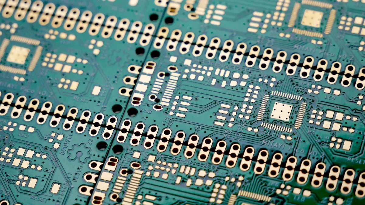
Outer Layer Processing in PCB Making
Adding Photoresist to Outer Layers
The first step is adding photoresist to the copper. Photoresist is a material that reacts to light. It helps create the circuit design on the board. Manufacturers use special tools to spread it evenly. If it’s uneven, the board might not work well.
PCB makers follow strict rules to ensure quality. For example, the board can’t bend more than 1%. Also, hole positions must stay within 0.003 inches. These rules help make sure the board matches the design.
Specification | Requirement |
|---|---|
Board bending limit | No more than 1% |
Hole position accuracy | Within 0.003 inches |
Board size tolerance | ±0.005 inches |
Line width variation | No more than ±0.025 mm or 20% |
Assembly bow and twist | Max 0.7% of longest side |
Layer alignment | Within ±2 mil tolerance |
Front-to-back alignment | Within 5 mil tolerance |
Using UV Light to Create Circuit Paths
Next, UV light shines on the photoresist. The light hardens some parts, leaving others soft. A special solution washes away the soft parts. This shows the copper underneath. This step makes the circuit paths clear and accurate.
Accuracy is very important here. If layers don’t match, the board won’t work. Advanced machines help align layers within ±2 mil. This ensures the board works as planned.
Removing Extra Copper from Outer Layers
The last step removes extra copper from the board. This leaves only the needed circuit paths. First, most copper is removed quickly. Then, smaller areas are etched carefully. Special tools focus on spots needing extra work. Machines check to make sure the copper is even.
Step | Description |
|---|---|
Removes most copper fast. | |
Careful etching | Slowly removes leftover copper for precision. |
Focused etching | Targets small areas needing extra attention. |
Checking results | Tools measure to confirm copper is even. |
These steps ensure the board is high-quality and works well.
Solder Mask and Silkscreen Application in PCB Manufacturing
Adding the Solder Mask
The solder mask is a layer that protects the PCB. It keeps copper parts safe from rust and stops short circuits. This layer helps the board last longer and work well. It also shows where soldering can happen, leaving pads and holes open for parts.
Manufacturers use a special liquid solder mask for accuracy. First, they cover the board with the material. Then, UV light hardens certain areas based on the design. Extra material is cleaned off, leaving a neat protective layer. This step is key to making a strong and long-lasting PCB.
Solder masks come in many colors, but green is most common. Other colors like red, blue, or black can also be used. The solder mask not only protects the board but makes it look better too.
Adding the Silkscreen Layer
The silkscreen layer adds labels and symbols to the PCB. It shows important details like part names, test spots, and logos. This makes it easier to find parts and fix problems later.
Different boards need different silkscreen methods. Hard boards use standard printing for clear labels. Flexible boards need stronger materials to handle bending. Boards for hot places, like in space or hospitals, use heat-proof inks or lasers. Industry rules make sure silkscreens are high quality.
The silkscreen layer makes the board look professional and easy to use. Picking the right materials and methods ensures the board works well and looks great.
Surface Finishing in PCB Fabrication
Adding a Protective Coating
A protective coating keeps your PCB safe from damage. It helps the board last longer and work better. Conformal coatings are often used to protect against water, dust, and rust. These coatings act like a shield, stopping wear and failure. This is especially important for devices like medical tools. Adding this layer makes the board stronger and more durable.
Different coatings have special benefits. For example, conformal coatings stop oxidation, which keeps the board working well. They also prevent rust, especially in wet or dirty places. This step is very important to make sure your PCB works well for a long time.
Benefit | How It Helps the Board |
|---|---|
Less Wear and Tear | Slows down damage over time |
Stops Failures | Lowers the chance of breaking |
Better Reliability | Lasts longer in tough conditions |
Tip: Pick a coating that fits your PCB's job and environment. This helps it work better and last longer.
Common Surface Finishes (e.g., HASL, ENIG)
Surface finishes protect copper and make soldering easier. Two common finishes are HASL (Hot Air Solder Leveling) and ENIG (Electroless Nickel Immersion Gold). HASL is cheaper and good for simple parts. ENIG costs more but works well for detailed designs.
ENIG lasts longer and stops rust, making it great for important uses. It also creates strong solder joints, which help the board work well. HASL is less expensive but has a rougher surface and doesn’t last as long. ENIG is better for eco-friendly projects because it follows RoHS rules, while HASL may have lead.
Feature | HASL | ENIG |
|---|---|---|
Cost | Less expensive | More expensive |
Surface Smoothness | Rough | Smooth |
Soldering | Good for basic parts | Best for small details |
Environmental Impact | May have lead | Lead-free (RoHS safe) |
Durability | Shorter lifespan | Longer lifespan |
Picking the right surface finish helps your PCB last longer. It also ensures the board works well in its specific use.
Testing and Final Inspection in PCB Manufacturing
The last steps in making a PCB check its quality. These include electrical tests, visual checks, and quality assurance. Each step ensures the PCB works well and meets standards.
Electrical Testing for Continuity and Shorts
Electrical testing makes sure the PCB works correctly. It checks that electricity flows through all paths without stopping. It also finds shorts, where wrong connections could cause problems.
Special machines like flying probe testers or bed-of-nails testers are used. These machines test every path and hole on the board. For complex boards, automated systems make testing faster and more accurate.
Tip: Electrical testing finds hidden problems that you can’t see. It ensures the PCB works properly in real use.
Visual Inspection for Defects
Visual inspection looks for surface problems on the PCB. This step checks if the board is clean and matches the design. Technicians look for scratches, misplaced parts, or bad solder joints.
Automated optical inspection (AOI) systems use cameras to find flaws. These systems can spot problems like solder bridges or missing parts. For layered boards, X-ray machines find hidden issues like gaps in solder or misaligned layers.
Why visual and automated inspections are helpful:
Finds surface problems early.
Checks alignment and solder quality.
Makes the PCB more reliable.
Quality Assurance and Packaging by LT CIRCUIT
Quality assurance is the final check in making a PCB. Here, results are recorded, and the board is checked against industry rules. LT CIRCUIT uses strict quality controls to make dependable PCBs.
Important quality checks include functional testing. This simulates real-world use to ensure the PCB works as planned. After testing, the board is carefully packed to avoid damage during shipping.
Inspection Method | How It Helps Quality |
|---|---|
Visual and automated optical inspection | Finds surface flaws and ensures the board looks good. |
X-ray inspection for hidden joints | Spots internal problems not visible on the surface. |
Electrical testing | Confirms the PCB works as designed. |
Functional testing | Tests the PCB in real-world conditions. |
Careful checks and quality assurance lower the chance of defects. Regular inspections improve PCB quality and keep customers happy. With LT CIRCUIT’s high standards, you can trust their PCBs to perform well.
Making a PCB involves careful steps, from start to finish. Each step checks that the board meets strict standards. Accuracy and quality checks are very important for good results. LT CIRCUIT uses smart tools and strict rules to make great PCBs. You can count on them to meet your needs.
FAQ
What does a solder mask do on a PCB?
The solder mask keeps copper safe from rust and stops short circuits. It also makes the board stronger and improves how it looks.
Why is aligning layers important in making PCBs?
Good alignment makes sure all layers connect properly. If layers don’t match, the PCB might fail and not work well.
How does LT CIRCUIT make sure PCBs are high quality?
LT CIRCUIT checks PCBs with special tests like electrical checks, visual reviews, and real-use simulations. These steps make sure the PCBs are strong and work reliably.
See Also
Understanding The Materials Used In Printed Circuit Boards
Exploring The Manufacturing Steps For Rigid-Flex PCBs
Key Stages In Efficient Turnkey PCB Assembly Process
Defining PCB Printed Circuit Boards And Their Fundamental Ideas
Challenges In Prototyping And Manufacturing Multi-Layer Circuit Boards