Mastering the Art of PCB Manufacturing with Press-Fit Holes
Press-fit holes play a crucial role in the manufacturing of modern PCBs, offering a reliable method for creating connections without the need for solder. This innovative approach is rapidly gaining traction within the industry. The press-fit connectors market is projected to reach $9.91 billion by 2024 and could grow further to $15.87 billion by 2033. Precision is essential for ensuring the effectiveness of press-fit holes in PCBs, requiring careful attention to hole size, shape, and wall strength. These factors are critical in preventing issues and maintaining robust connections during assembly.
Key Takeaways
Press-fit holes connect parts in PCBs without solder. This makes assembly faster and lowers heat damage to parts.
The hole size must be correct for a good fit. Make holes 0.007 inches bigger than the lead size for a tight connection.
Share clear details with your PCB maker about designs. Include hole sizes and plating info to avoid mistakes and get great results.
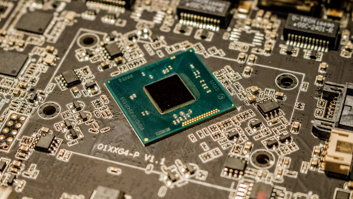
Understanding Press-Fit Holes in PCB Manufacturing
Definition and Key Features
Press-fit holes are special openings in PCBs for press-fit parts. These parts fit into the holes without needing solder. This creates a strong and reliable electrical link. The process depends on how well the pins fit the hole walls. This fit ensures a solid bond and good conductivity.
Press-fit holes follow rules like DIN/IEC 60352-5 for quality. Hole sizes are usually between 0.8 mm and 1.6 mm. They can handle high heat, up to 125 °C or 150 °C. Special materials and coatings stop problems like chips or whiskers. These features make them great for modern PCB designs.
Advantages of Solder-Free Connections
Not using solder has many benefits over old methods. Here’s a simple table of its perks:
Advantage | Description |
|---|---|
Reliability | More reliable than soldering connections. |
Speed of Assembly | |
Mechanical Retaining Force | Strong hold keeps connections stable. |
Double-Sided Mounting | Parts can go on both sides of the PCB. |
No Thermal Stress | No heat damage during assembly. |
Without solder, there’s no heat stress on parts. This protects delicate components. The process is also quicker, saving time and money. Strong holding power keeps connections steady, even in tough conditions.
Applications in Modern Electronics
Press-fit holes are key in today’s electronics because they’re reliable. They are used in many areas, such as:
Automotive Electronics: Handle heat and shaking, perfect for car systems like engines.
Telecommunications: Help with fast data in servers and network tools.
Consumer Electronics: Used in phones and laptops for strong, small connections.
Industrial Equipment: Improve reliability in factory machines and automation.
Their ability to work on both sides and in tough conditions makes them essential. They adapt well to the needs of modern technology.
Designing PCBs with Press-Fit Holes
Hole Size and Tolerance Requirements
When making PCBs with press-fit holes, hole size matters a lot. The size and tolerance affect how well the parts fit. A good rule is to make holes 0.007 inches bigger than the lead size. This extra space helps with drill wear and plating changes, ensuring a snug fit.
Manufacturers set exact tolerances to keep things consistent. For plated holes, the tolerance is usually ±0.003 inches. For non-plated holes, it’s ±0.002 inches. Here’s a table showing common tolerances:
Hole Type | Tolerance |
|---|---|
Plated Holes | ±0.003 inches |
Non-Plated Holes | ±0.002 inches |
Using tools like Altium Designer® can help you plan better. These tools let you add hole size details to your design files for clear instructions.
Tip: Always include tolerance details for pads and vias. This ensures parts fit perfectly during assembly.
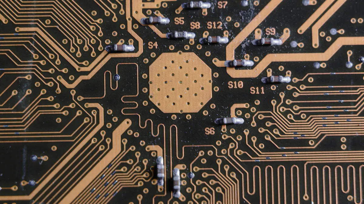
Plated-Through-Hole (PTH) Specifications
Plated-through-holes (PTHs) are very important for press-fit parts. They connect different layers in a PCB and must meet certain standards. Key factors include:
Parameter | Importance |
|---|---|
Drilling accuracy | Keeps holes straight and aligned. |
Drill bit quality | Affects smoothness and plating stickiness. |
Hole wall pretreatment | Cleans walls for even plating. |
Plating solution chemistry | Impacts copper quality and plating speed. |
Plating current density | Controls thickness and plating shape. |
Plating temperature | Affects copper strength and flexibility. |
Plating thickness uniformity | Prevents weak spots or open circuits. |
Good PTH specs improve conductivity and make connections stronger. Thick copper plating lowers resistance and handles heat better. Even plating avoids problems like gaps or thin spots that could weaken the PCB.
Pad Design and Solder Mask Considerations
Pads and solder masks are key for press-fit holes. Pads need strong rings to avoid breaking during drilling. The solder mask must not block the press-fit process.
Here are some tips for pad and solder mask design:
Best Practice | Description |
|---|---|
Annular rings | Prevent pad damage during drilling. |
Vias | Design for better electrical flow. |
Trace width and space | Follow rules for easier manufacturing. |
Solder mask and silkscreen | Apply carefully for smooth assembly. |
Following these tips makes PCBs stronger and more reliable. Good pad design keeps press-fit parts secure and working well.
Communicating Design Needs to Manufacturers
Sharing clear details with your PCB maker is very important. Include hole sizes, PTH specs, and pad designs in your files. This helps the manufacturer understand your needs and make accurate PCBs.
Tools like Altium Designer® can help you organize your design. Add a drill holes table with tolerances for each hole type. This reduces mistakes and confusion during production.
Note: Working with experts like LT Circuit makes this easier. They know how to make high-quality PCBs for reliable press-fit parts.
Fabrication and Quality Control by LT CIRCUIT
Precise Drilling for Reliable Connections
Drilling is key to making press-fit holes work. Accurate drilling keeps holes aligned with press-fit parts. LT CIRCUIT uses advanced CNC machines for perfect drilling. These machines make smooth walls and exact hole sizes. Smooth walls help with plating and strong connections. Burrs are reduced, ensuring the holes are ready for assembly. LT CIRCUIT focuses on precision to meet strict press-fit standards.
Tip: Check your design files for correct drilling details. This avoids mistakes during production.
Surface Finishing and Plating Options
Plating and finishes are important for making strong PCBs. LT CIRCUIT offers different finishes to match your needs. Each finish has pros and cons, as shown below:
Surface Finish Type | Benefits | Drawbacks |
|---|---|---|
HASL | Cheap, sticks well | Rough surface, not good for tiny parts |
ENIG | Protects from rust, great for small parts | Costs more |
OSP | Eco-friendly, affordable | Short shelf life, needs careful handling |
ISn | Flat surface, good for small parts | Can rust over time |
IAg | Easy to solder, smooth finish | Can tarnish, short storage life |
LT CIRCUIT ensures even plating thickness. This avoids weak spots and keeps electrical connections strong. Careful finishing makes PCBs work well in different conditions.
Checking Hole Accuracy
Inspecting holes is crucial for quality control. LT CIRCUIT uses optical and X-ray tools to check hole size and placement. These tools find tiny errors to match your design specs. Automated checks reduce mistakes and improve reliability. Accurate inspections ensure your PCBs meet high standards.
Note: Regular checks during production catch problems early. This saves time and money.
Testing Plating for Electrical Strength
Good plating is vital for strong electrical performance. LT CIRCUIT uses tests to check plating quality. These include:
Test Type | Purpose |
|---|---|
Four-Point Probe Test | Measures resistance for conductivity accuracy. |
Eddy Current Testing | Finds flaws and checks coating thickness. |
Salt Spray Test | Tests resistance to rust for long-term use. |
Thermal Cycling | Checks plating under extreme temperatures. |
Humidity Resistance | Tests how moisture affects electrical properties. |
UV Exposure Testing | Simulates sunlight effects for durability. |
These tests ensure plating stays strong in tough conditions. LT CIRCUIT delivers PCBs that work reliably in demanding environments.
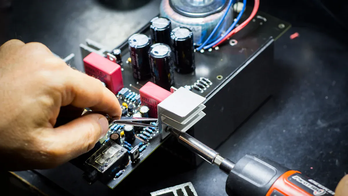
Assembly Process for Press-Fit Holes
Controlled Insertion Techniques
Press-fit assembly needs careful handling for strong connections. You must use the right amount of force to push parts into the PCB without breaking anything. Machines are often used because they press parts evenly and correctly. These machines also lower mistakes that people might make, ensuring every connection is done properly.
To get the best results, watch the force and speed closely. Too much force can bend the pins or harm the holes. Too little force might make weak connections. Special tools made for press-fit assembly help keep the process smooth and reliable.
Tooling and Alignment Best Practices
Good tools and alignment are key to protecting the PCB during assembly. Tooling holes help place the board correctly in machines. They also align stencils for solder paste and hold the board steady when adding parts.
Aspect | Description |
|---|---|
Precision Manufacturing | Automated systems like SMT and THT ensure accuracy in complex designs. |
Quality Assurance | Inspections like AOI and X-ray catch defects early. |
By using these methods, you can reduce mistakes and improve the assembly's quality.
Preventing PCB Damage During Assembly
Keeping the PCB safe from damage is very important for a reliable product. Studies, like those by MS ELECTROVISION PVT LTD, show how checking for risks at each step helps. Follow these steps to avoid damage:
Test and inspect to gather useful details.
Study the problem to fix it and stop it from happening again.
These steps help catch problems early and fix them before they grow worse.
Importance of Press Head Selection
The press head is a key part of press-fit assembly. Picking the right press head spreads the force evenly when pressing parts in. A good press head lowers stress on the PCB and avoids breaking parts. Make sure the press head fits the size and shape of the connectors for the best results.
Also, keep the press head in good condition with regular care. A worn-out press head can press unevenly and cause bad connections.
Tip: Talk to your PCB maker to check if the press head matches your assembly needs.
Making PCBs with press-fit holes needs careful work and planning. You must drill holes correctly, plate them well, and assemble parts carefully. New tools, like AI systems, help find mistakes fast. They also fix problems while making the PCBs. These smart tools show why fixing errors early is important. Working with experts like LT CIRCUIT helps you use the best methods. This teamwork makes strong and reliable PCBs for today’s needs. Following these steps ensures your press-fit designs work perfectly.
FAQ
What are press-fit holes in PCBs?
Press-fit holes are special spots in PCBs. They hold parts tightly without solder. This makes strong and steady electrical links.
How do press-fit holes improve PCB assembly?
They skip soldering, cutting down heat damage and saving time. This method makes connections strong and allows parts on both sides.
Why choose LT CIRCUIT for press-fit PCBs?
LT CIRCUIT uses exact drilling, top-notch plating, and strict checks. They make high-quality PCBs for today’s technology needs.
See Also
Understanding Press-Fit Holes in Printed Circuit Boards
An In-Depth Look at PCB Fabrication Techniques
Tips for Smoother Electroplating in HDI PCB Holes
Challenges in Manufacturing and Prototyping Multi-Layer PCBs