PCB Manufacturing Process
Printed circuit boards (PCBs) are key parts of electronics today. Without PCBs, gadgets like phones, computers, and medical tools wouldn't work. The need for PCBs is increasing every year, driven by advancements in the PCB manufacturing process. The global market may grow from $78.5 billion in 2023 to $120 billion by 2032. This growth shows how important making PCBs is for new ideas and better technology.
Key Takeaways
Learning about PCBs, like single-sided, double-sided, and multilayer, helps you pick the best one for your project.
Using a good design process, like making schematics and layouts, makes sure your PCB works well and is high quality.
Using eco-friendly methods in PCB making lowers harm to nature and supports recycling, which helps the Earth and your project.
Learning About Printed Circuit Boards
Printed circuit boards (PCBs) come in different types. Each type is made for a specific purpose. Knowing these types helps you pick the best one for your project.
Single-Sided PCBs
Single-sided PCBs are the easiest to make. They have one layer of conductive material. This makes them great for simple circuits. They use fewer materials and take less time to make. These PCBs are the cheapest option. You can find them in basic devices like calculators and power supplies.
Double-Sided PCBs
Double-sided PCBs have conductive layers on both sides. This lets you add parts to either side. It makes the circuit more complex. These PCBs are used in things like LED lights and car dashboards. They are good for medium-level designs.
Multilayer PCBs
Multilayer PCBs have many layers of conductive material. Insulating layers keep them apart. They are used for small, complex circuits. Devices like smartphones and medical tools need these PCBs. They work well but are harder to make.
Rigid PCBs
Rigid PCBs are made from hard materials that don’t bend. They are strong and last a long time. Over 70% of makers use rigid-flex PCBs in electronics. Cars, including electric ones, use them a lot. They are also popular in aerospace and telecom industries.
Flexible PCBs
Flexible PCBs are made from materials that can bend. They are great for wearable gadgets and small devices. The market for flexible PCBs is growing fast. It might reach $13.96 billion by 2025 and $17.81 billion by 2033. Their flexibility helps create cool new designs.
PCB Design Process
Making a printed circuit board (PCB) needs careful planning. Each step builds on the one before it. Following the steps in order is very important.
Schematic Design
The schematic design is like a map for your PCB. It shows how parts connect and work together. This step makes sure your design fits your project’s needs.
Tip: Knowing what your project needs early saves time and money later.
To make this step easier and more accurate, try these tips:
Follow rules like IPC-2221 for trace width and copper thickness.
Plan layer order and handle cutouts carefully to avoid problems.
A good schematic saves time and prevents mistakes. For example, bad data can cause big delays, as shown below:
Problem Type | What Happened | Result |
|---|---|---|
Design Delays | Poor data caused many delays for Company X. | Project was late with no prototypes ready. |
Rework Time | Fixing data issues took over 3 weeks. | Helped stop more delays later. |
Cost Increase | Bad data raised manufacturing costs. | Costs went up by 5-10%. |
Project Success | Good data led to on-time project completion. | Project finished on time with no issues. |
Risk of Failures | Bad data increased chances of problems later. | 2-3X more likely to face failures. |
By using accurate data and following rules, you can make a better schematic and avoid problems.
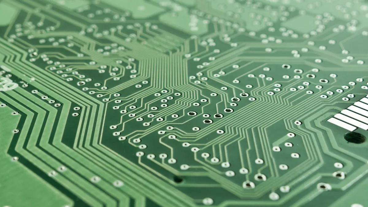
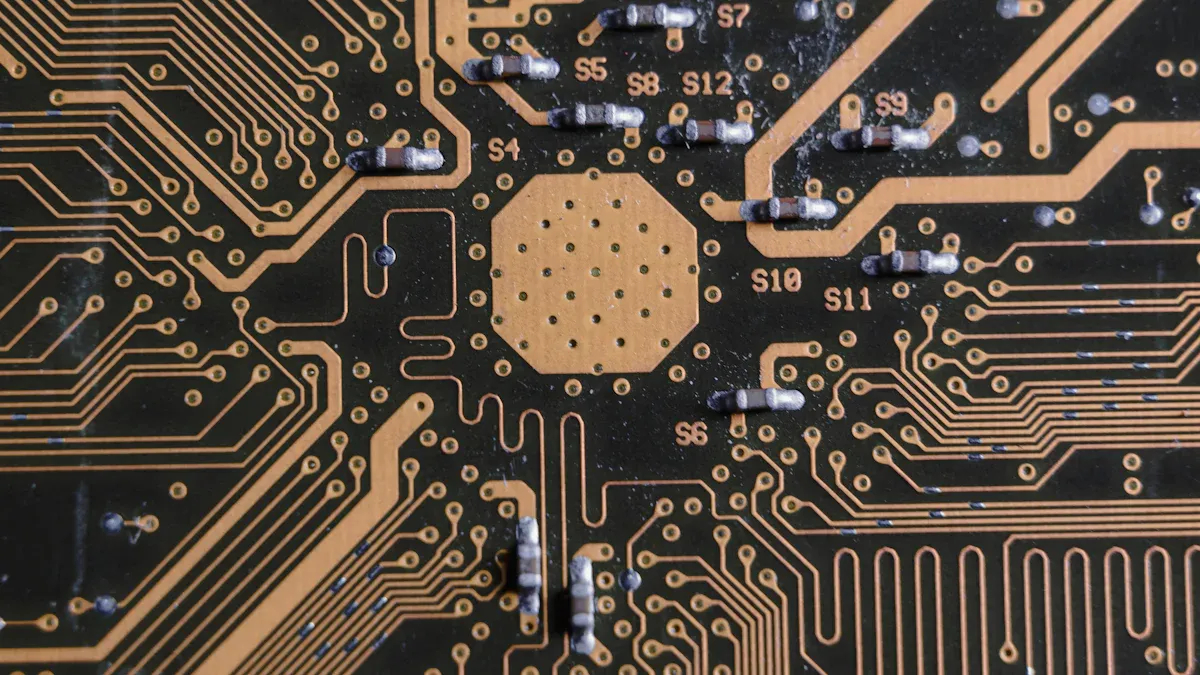
PCB Layout
The PCB layout turns your schematic into a real design. This step places parts and connects them with traces. A good layout helps your PCB work well and last longer.
Good PCB layouts have these features:
Fit more parts on smaller boards.
Reduce signal problems with ground and power planes.
Manage heat better using thermal vias and copper planes.
Here are more ways to improve your PCB layout:
Feature | How It Helps |
|---|---|
Complex Routing | Makes it easier to connect many layers. |
Impedance Matching | Keeps signals steady between source and load. |
Crosstalk | Stops signals from interfering with each other. |
Grounding | Reduces noise by giving a stable ground. |
Trace Layout | Keeps signals clear, especially for fast ones. |
Heat Sinks | Removes heat from powerful parts. |
Component Placement | Puts hot parts where heat can escape easily. |
Using these ideas will make your PCB layout better and more reliable.
Design for Manufacturability (DFM)
Design for Manufacturability (DFM) makes sure your PCB is easy to build. It finds problems that could slow down production.
Statistics are very helpful in DFM. They show patterns and help fix issues. For example:
Statistics can find unusual problems in your design.
These insights improve testing and lower risks.
Adding DFM ideas to your design lowers costs and improves quality. Fixing manufacturability early makes production faster and smoother.
Step-by-Step PCB Manufacturing Process
Printed circuit boards (PCBs) are made through several careful steps. Each step is important to make sure the final board works well and meets quality standards. Let’s break down the process.
Imaging and Film Creation
Imaging is the first step in making a PCB. The design is copied onto a film, which acts like a guide. Special materials that react to UV light are used to create the film. When exposed to light, these materials harden into the circuit pattern.
Tip: Make sure the film lines up perfectly with the PCB base to avoid mistakes later.
Etching and Copper Removal
Etching takes away extra copper from the PCB surface. This leaves only the needed circuit paths. Most manufacturers use chemicals to do this. The chemicals remove unwanted copper but keep the design intact. Precision is very important here because small mistakes can ruin the circuit.
Etching removes extra copper, leaving only the needed parts.
Machines like Automated Optical Inspection (AOI) check the etched patterns for errors.
Controlling chemical strength and temperature helps avoid defects.
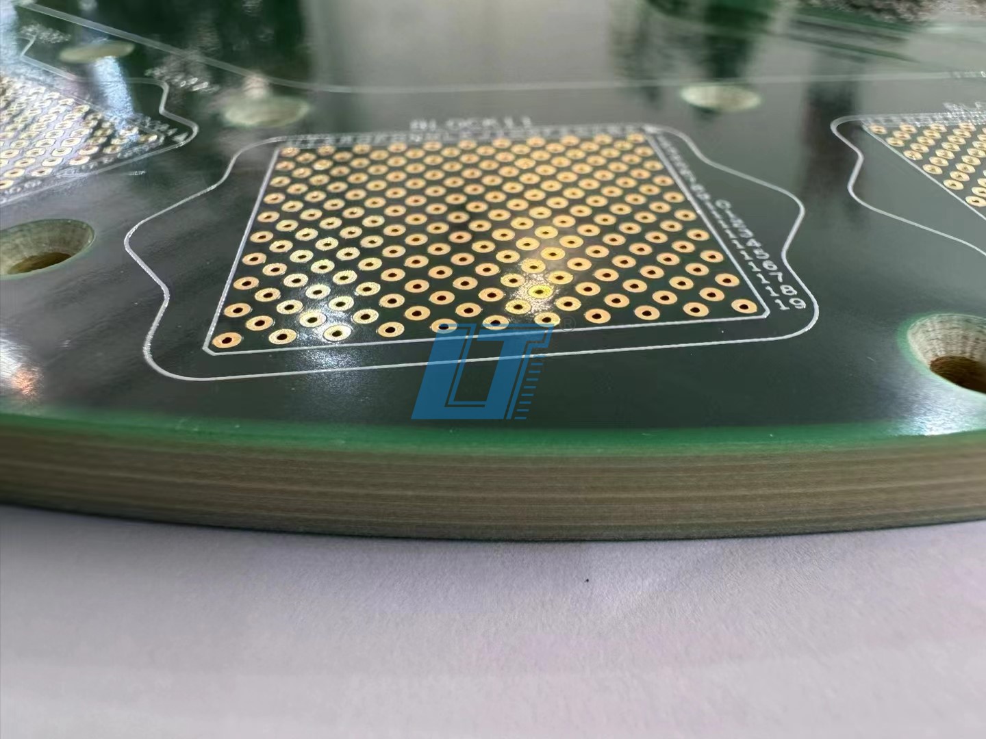
Drilling and Hole Formation
Drilling makes holes for parts and electrical connections. Special machines are used to drill with great accuracy. Proper drilling is key to making a reliable PCB.
Use quality checks to monitor the drilling process.
Test drill accuracy with tools like measuring machines.
Check holes for rough edges or uneven shapes.
Measure hole depth with depth gauges.
Keep records to fix repeated problems.
Train workers to use advanced machines correctly.
Drilling affects how well the PCB works. Better tools and methods improve accuracy and quality.
Plating and Layer Bonding
Plating adds a thin copper layer to holes and circuits. This improves conductivity and strengthens the PCB. Layer bonding uses heat and pressure to join multiple PCB layers together.
Modern plating is tested with heat and shock tests. Good plating shows less than a 10% resistance change after 1000 hours of testing. This ensures the PCB works well in tough conditions.
Solder Mask Application
The solder mask protects copper circuits from damage and short circuits. It is applied using special techniques like photolithography. A good solder mask prevents problems like missing shields or solder balls.
IPC rules guide solder mask application to keep PCBs strong.
Balanced processes lower the chance of missing solder masks.
Silkscreen Printing
Silkscreen printing adds labels and markings to the PCB. These help identify parts and connections during assembly. Different methods offer various levels of accuracy and cost.
Technique | Benefits | Drawbacks |
|---|---|---|
Manual Screen Printing | Cheap, easy for small jobs, quick setup. | Less accurate, not good for detailed designs, quality may vary. |
Liquid Photo Imaging (LPI) | More precise, good for complex designs, better resolution. | Slower, more expensive, not ideal for very tiny features. |
Direct Legend Printing (DLP) | Most accurate, great for complex PCBs, no waste. | Expensive machines, usually used for long production runs. |
Electrical Testing and Inspection
Electrical testing checks if the PCB works before assembly. Different methods are used to find problems and ensure reliability.
Automated Optical Inspection (AOI): Spots assembly mistakes and gives pass/fail results.
Continuity and Hi-Pot Tests: Check electrical connections and insulation strength.
PCB Stress Testing: Includes vibration and heat tests to see if the PCB can handle tough conditions.
Careful testing ensures the PCB meets standards and works well in real-world use.
PCB Assembly Process
The PCB assembly process turns a bare printed circuit board into a working electronic part. It includes placing components, soldering them firmly, and checking everything to ensure it works well.
Component Placement
Component placement is the first step in assembling a PCB. Electronic parts must be placed correctly on the board to work properly. Machines do this job with great accuracy, using fiducial markers to align parts perfectly. These machines have improved a lot over time. For example:
Year | AI Use in Machines | Accuracy Growth | Defects Found |
|---|---|---|---|
2004 | None | Basic | Few |
2010 | 33% | Better | More |
Over 50% | Excellent | Many |
Placing parts smartly helps manage heat and improves performance. This step is very important for making durable PCBs, especially for advanced devices.
Tip: Using Design for Assembly (DFA) rules can reduce mistakes during this step.
Soldering Techniques
Soldering connects parts to the PCB, creating strong electrical paths. Different methods are used based on how complex the project is. Each method has pros and cons:
Soldering Method | Benefits | Downsides |
|---|---|---|
Wave Soldering | Reliable; Good for many connections. | Not great for complex designs. |
Hand Soldering | Precise; Good for small fixes. | Slow; Can have human errors. |
Reflow Soldering | Accurate; Automated for consistency. | Needs setup and calibration. |
Selective Soldering | Focuses on specific spots. | Costs more for equipment. |
Reflow soldering is the most popular method today because it’s precise and automated. Good soldering is key to avoiding problems, as bad connections can lead to failures.
Final Inspection and Testing
The last step checks if the PCB meets quality standards. Tests and inspections confirm that every part works as it should. The process usually includes:
Step | What Happens |
|---|---|
1 | Check all test and inspection results. |
2 | Confirm traceability records. |
3 | Do a final visual check. |
4 | Inspect packaging. |
5 | Test random samples if needed. |
Automated Optical Inspection (AOI) and functional tests find issues like misplaced parts or bad soldering. These checks make sure the PCB works well in real-world situations.
Note: Careful inspections lower the chance of defects, saving time and money later.
Quality Control in PCB Manufacturing
Quality control makes sure every pcb works well and meets standards. Careful testing and inspections help find problems early. This improves the quality of your boards.
Electrical Testing for Defects
Electrical testing checks for broken circuits, shorts, and bad connections. It uses methods like in-circuit testing (ICT) and functional testing. ICT looks at each part, while functional testing checks if the pcb works in real-world use. Hi-Pot tests measure insulation strength to stop electrical failures. These tests catch issues before assembly, saving time and money.
Tip: Testing often lowers the chance of defects and keeps your pcb reliable.
Visual and Automated Inspections
Visual and automated checks find physical problems on the pcb. Automated Optical Inspection (AOI) uses cameras to spot misplaced parts or soldering mistakes. Dimensional checks make sure the pcb matches its design. Reflow soldering inspections confirm solder joints are strong. Combining manual and automated checks improves accuracy and consistency.
Quality Control Benchmark | What It Does |
|---|---|
Reflow Soldering | Checks solder joints with heat profiles and visual tests. |
Automated Inspection | Finds placement errors and bad solder joints. |
Dimensional Inspections | Uses AOI to check the pcb size and shape. |
Environmental Stress Testing
Stress testing shows how tough the pcb is in real-world conditions. Thermal cycling tests extreme temperature changes. Vibration tests check if the pcb can handle shaking or movement. These tests ensure the pcb works in harsh places like cars or planes. Following rules like IPC-A-600 keeps quality consistent. Stress tests find weak spots and improve the design for long-term use.
Note: Stress tests make sure your pcb works well in tough environments.
Environmental Considerations in PCB Manufacturing
Waste Management Practices
Making PCBs can create waste that harms nature. Managing this waste helps keep the environment safe. Treating wastewater removes bad chemicals from water used in production. Filters clean the water before it goes back to nature. Recycling old electronics stops harmful disposal and saves useful materials.
Using lean manufacturing reduces waste by improving processes. This method cuts down on extra materials and energy use. Following strict rules helps limit dangerous substances during production. Extended Producer Responsibility (EPR) makes companies handle their products’ disposal and recycling.
Here’s a list of waste management strategies:
Strategy | What It Does |
|---|---|
Wastewater Treatment | Filters clean water used in PCB production. |
E-waste Recycling Programs | Collects old electronics to stop bad disposal. |
Regulatory Compliance | Limits harmful materials with strict rules. |
Waste Reduction Initiatives | Cuts waste by improving production methods. |
These practices lower pollution and help protect the planet.
Sustainable Manufacturing Solutions
Sustainable manufacturing reduces harm to the environment. Using safer materials replaces toxic ones. Green methods make less dangerous waste and keep workers safe. Design for Environment (DfE) creates PCBs that are easier to recycle. This helps reduce the impact of products on nature.
Recycling old PCBs saves parts and lowers the need for new materials. These methods use less energy and cut greenhouse gas emissions. Energy-efficient processes also reduce power use during production. Sustainable practices protect nature and save money.
Here’s a summary of sustainable solutions:
Strategy | What It Does |
|---|---|
Green Manufacturing | Uses safer materials to lower harmful waste. |
Design for Environment (DfE) | Makes PCBs easier to recycle with eco-friendly designs. |
Advanced Recycling Technologies | Saves parts from old PCBs to reduce raw material use. |
By using sustainable methods, PCB production can meet environmental goals and stay high-quality.
Choosing LT CIRCUIT for Your PCB Needs
If you need printed circuit boards, LT CIRCUIT is a great choice. They focus on quality, new ideas, and happy customers. LT CIRCUIT makes sure your pcb needs are handled with care.
Why Pick LT CIRCUIT?
LT CIRCUIT has many benefits that make it a top pick:
Advanced Technology: They use modern tools to make strong pcbs. This ensures every product works well and lasts long.
Customization Options: Whether you need a simple or complex pcb, they can help. LT CIRCUIT creates designs that match your exact needs.
Fast Turnaround Times: Their quick processes deliver pcbs fast without losing quality.
Did You Know? LT CIRCUIT makes HDI pcbs, perfect for small, powerful devices like phones and medical tools.
Certifications and Quality Standards
LT CIRCUIT follows strict rules to ensure top-quality products. They have certifications like ISO 9001 and IPC-A-600. These prove their commitment to making excellent pcbs. With LT CIRCUIT, you can trust your boards will work well in any device.
Customer Support and Custom Designs
LT CIRCUIT values its customers and offers great support. Their experts help you design the perfect pcb for your project. They also offer many custom options, like different solder mask colors and finishes. You can even choose special testing services. This flexibility helps you create a pcb that fits your needs.
Tip: Contact LT CIRCUIT’s support team for advice on the best materials and designs for your pcb.
Making PCBs is key to building reliable electronics today. Every step ensures accuracy and quality for smooth device performance. Choosing eco-friendly methods and a trusted maker like LT CIRCUIT helps create top-quality PCBs while protecting the environment.
FAQ
How long does a PCB last?
A PCB’s lifespan depends on how it’s used and where it’s kept. Most PCBs can work for 10-20 years if cared for and used in normal conditions.
How do you pick the best PCB for your project?
Think about your device’s needs, like size and complexity. Flexible PCBs are great for wearable gadgets. Multilayer PCBs work well for advanced devices like smartphones.
Are PCBs recyclable?
Yes, PCBs can be recycled! Recycling saves materials like copper and gold. It also helps reduce electronic waste, which is better for the environment.
Tip: Look into local recycling programs to safely dispose of PCBs. ♻️
See Also
Understanding The Comprehensive Process Of PCB Fabrication
Exploring The Manufacturing Steps For Rigid-Flex Circuit Boards
Challenges And Processes In Multi-Layer Circuit Board Production