PCB Silkscreen Printing Process Precision Standards
You must maintain strict physical metrics to guarantee optimal legibility and yield during automated assembly. The pcb silkscreen printing process demands precise geometric controls to prevent production defects.
Parameter | Precision Standard |
|---|---|
Minimum Character Height | 0.8–1.0 mm |
Minimum Line Width | 0.1–0.15 mm |
Line-to-Line Clearance | 0.15 mm |
Pad Clearance | ≥0.15 mm |
Alignment Tolerance | ±0.1 mm |
Adhering to these pcb standards prevents solderability failures and component misalignment. You also eliminate optical inspection errors during automated SMT placement. Precise silkscreen alignment keeps ink off active pads and maintains crucial legend clarity across every board design.
Key Takeaways
Keep the letter height at least 0.8 millimeters tall so the text is easy to read.
Leave a tiny gap of at least 0.15 millimeters between the printed text and the metal pads.
Use Direct Legend Printing to get exact line thickness and neat, close positioning.
Leave more space around text on thick copper circuit boards so the ink does not bleed.
Review your design files early so automatic software tools do not cut off important text.
PCB Silkscreen Printing Technologies
Comparing DLP and Liquid Photo Imaging
Your choice of board manufacturing method depends on design details and your total budget. Standard screen printing keeps tooling costs low for large production runs. Even so, modern pcb silkscreen printing requires much tighter precision standards. Liquid Photo Imaging (LPI) spreads liquid photo-imageable ink over the board before UV light exposure. This liquid technique gives great resolution accuracy for detailed, packed printed circuit board designs.
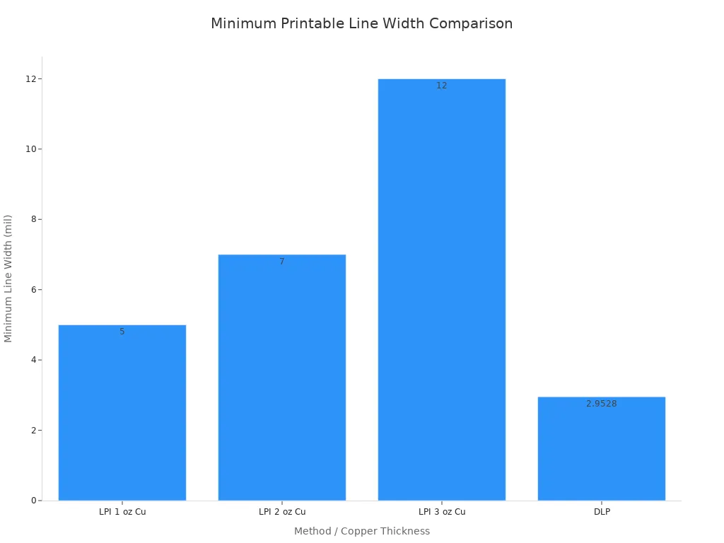
Direct Legend Printing (DLP) uses digital inkjet heads with fast UV-LED light curing. DLP removes the need for physical artwork screens and stencils completely. This fresh silkscreen printing technology creates a sharp minimum printable line width of 3 mil. Meanwhile, LPI performance relies mostly on the board's copper weight. LPI makes a 5 mil line width on 1 oz copper layers. Thicker copper needs wider legend lines to stop ink from pooling or smudging.
Layer Registration Accuracy and Alignment
You get the clearest visual details by using precise optical machine alignment. Old manual screen printing gives a loose registration alignment tolerance of about 5 mil. Newer high-precision printing gear scans optical target marks directly on the board surface. DLP digital printing lines up every legend mark with copper traces underneath. This automated approach enhances pcb silkscreen edge quality on crowded board designs.
Correct layer alignment stops ink from bleeding onto active component solder pads. Manual screen printing needs a 5 mil non-via pad clearance gap. LPI lowers this clearance space down to 4 mil. DLP reaches a small 3 mil non-via pad clearance limit. You must position silkscreen design files carefully to avoid soldering problems during assembly. Quality pcb silkscreen printing guards bare copper areas during SMT reflow. Great pcb manufacturing depends on clear component labels. Picking the best silkscreen printing technology stops legend errors and ensures readable pcb silkscreen text.
Precision Standards for Silkscreen Printing Process
You must control geometric variables to meet rigorous pcb manufacturing criteria. High quality standards ensure clear text definition on every board design. The modern silkscreen printing process requires strict adherence to aspect ratios and physical material properties. You avoid costly automated optical inspection failures when you follow these proven industry rules. Careful layout setup preserves design intent across production runs. You achieve consistent quality when your physical measurements match exact manufacturing tolerances.
Character Height and Line Width Ratios
You maintain legend legibility during automated SMT assembly by selecting proper text dimensions. Machine vision cameras scan text quickly on busy circuit boards. Small text blurs when the ink stroke width is too thick relative to character height. Design rules specify clear geometric limits for minimum character height and line thickness.
Source | Recommended Width-to-Height Ratio | Minimum Character Height | Minimum Stroke Width | Interpretation |
|---|---|---|---|---|
Aivon | 1:5 to 1:6 | 1.0 mm / 40 mil | 0.15 mm / 6 mil | Preferred range for maximum visual legibility during optical scanning. |
Weller PCB | 1:6 | 1.0 mm / 40 mil | 0.15 mm / 6 mil | Conservative minimum baseline ratio for clear text output. |
You achieve optimum character resolution by applying a stroke width equal to one-sixth of the total character height. For example, a 1.0 mm character height requires a 0.15 mm stroke width. You prevent ink bleeding across small text openings with this balanced proportion. Wider letters like 'W' or 'M' need adequate interior spacing to prevent filled gaps. You maintain high visual contrast by enforcing these strict dimensional relationships.
You must keep legend ink completely off bare copper pads. Industry assembly practices require a clean placement strategy across the entire board layout. Automated computer-aided manufacturing clipping tools remove overlapping artwork errors before printing starts. However, you should design your silkscreen layer accurately from the very start of your project to ensure high assembly yields.
Substrate Material and Copper Weight Impacts
Your choice of base laminate directly affects overall print crispness and legend retention. Crucial pcb substrate considerations include surface roughness, laminate curvature, and material outgassing during thermal curing cycles. Rigid FR-4 laminates offer a flat, uniform surface for accurate digital ink deposition. Flexible substrates stretch under high heat. You must recalibrate machine alignment parameters when printing legends on flexible base materials. Proper material selection prevents ink adhesion loss during subsequent assembly steps.
Heavy copper traces present another physical challenge for the silkscreen printing process. Thick copper layers create tall topography steps across the pcb surface. Liquid ink naturally flows down steep copper edges into deep trace valleys. You get uneven line widths and visual text distortion over heavy copper features.
High copper weights require increased spacing around legend text to prevent ink pooling along steep trace edges.
You resolve surface height variations by adjusting your legend clearance values in your CAD software. Heavy copper designs demand wider minimum line widths than standard thin copper boards. You protect overall product reliability by evaluating pcb substrate considerations during early layout stages. Proper spacing keeps your pcb markings readable after board exposure to intense thermal reflow environments.
DFM Rules for PCB Silkscreen Clearance
Good DFM rules for pcb silkscreen printing will raise your production yield. Design for Manufacturing guidelines keep your board legend clear and simple to read. You should check main design considerations for pcb silkscreen parts when setting up your layout. Leaving correct physical spacing stops ink from dirtying open solder joints during hot reflow.
Solder Pad Clearance and Line Separation
You must place adjacent legend strokes far enough apart to stop text from blurring on circuit boards. Rules from JLCPCB say separate character lines must keep a gap over 0.15 mm. Liquid ink spills across thin gaps if character lines rest too near each other. JLCPCB suggests a best clearance gap of 0.25 mm or more to boost overall build yield.
You must also keep legend markings far away from solderable pads and copper parts. Put legend ink onto active component pads, and you create bad solder joints plus build errors.
Clearance Pair | Minimum Distance |
|---|---|
Silkscreen to pads or vias | 5 mil |
Silkscreen to SMD pads, through-holes, and mask openings | 6 mil |
Silkscreen text to insulation or solder-mask layer | 4.5 mil |
Silk to copper pad (IPC-7351 standard) | 0.2 mm (8 mil) |
Silk to solder mask (IPC-7351 standard) | 0.2 mm (8 mil) |
Silk to copper trace (IPC-7351 standard) | 0.15 mm (6 mil) |
Automated CAM software enforces a strict solder mask precedence rule before production begins. CAM tools trim off any legend mark that reaches into a solder mask opening. Trimming marks like this keeps the solder pads clean and easy to use. Sadly, automated trimming can cut off important parts of your legend text. A component tag like 'R18' can easily change into 'R1' after the trim step. You should check your layout against solder mask openings so text does not disappear. Use these tips for optimizing silkscreen printing to keep all board text sharp and clear.
Polarity Designators and High-Density Rules
Crowded printed circuit board layouts need smart legend placement near tight components. Small parts like fine-pitch QFN or BGA chips leave almost no space on the pcb face. You must follow strict design rules when putting marks on packed circuit boards.
Dense-Board Silkscreen Rule | Recommended Value |
|---|---|
Minimum font size (polarity and reference designators) | ≥ 1.0 mm (optimal 1.2–1.5 mm) |
Extremely limited space minimum font height | 40 mils (1.016 mm) baseline; 50 mils (1.27 mm) preferred |
Minimum line width | ≥ 0.15–0.20 mm (5 mils / 0.127 mm minimum) |
Pad or via clearance for fine-pitch QFN/BGA | ≥ 0.15 mm (6 mils / 0.152 mm minimum) |
Polarity marks and pin-1 tags show workers how to place components right during SMT setup. You must keep polarity marks easy to see after setting components down. Automated CAM cleaning deletes any polarity symbol that touches a solder mask opening. That automatic wipe can erase a diode cathode line or a plus sign completely. Missing direction marks make it far easier to put components on backward during automated building. You should shift polarity marks outside component outlines instead of depending on CAM trim tools.
You get great pcb builds when reviewing design considerations for pcb silkscreen details early on. Putting clear labels on the silkscreen layer takes steady checks on space gaps. You keep readable text and correct component alignment across every batch by following these clear physical limits.
Material Hardness and Reliability in PCB Manufacturing
Ink Adhesion and Thermal Reflow Stress
You test special epoxy inks to make sure they resist chemicals well during factory production. Modern surface mount assembly exposes every board marking to extreme heating cycles. Peak temperatures during lead-free reflow testing often reach 260 °C under IPC-TM-650 Method 2.4.28 guidelines. Liquid photo-imageable inks and UV-curable polymers serve as main materials used in pcb silkscreen printing. Poorly cured text markings break, turn dark, or peel away from the base layer when temperatures shift fast.
You test actual ink strength by doing basic tape adhesion checks inside the laboratory. Workers press sticky tape down hard over printed text lines following IPC-TM-650 Method 2.4.1 rules. Pulling the tape straight up quickly proves if cured ink sticks tightly to the underlying solder mask layer. Using certified materials used in pcb silkscreen printing stops text peeling during hot wave soldering. High ink hardness keeps component labels clear even after scrubbing boards with harsh liquid cleaners.
Automated Optical Inspection Compliance
You tune automated optical inspection equipment to check final text quality right after component reflow. Modern camera systems compare finished circuit boards directly against your initial layout design files. Low visual contrast between dark solder mask backgrounds and bright text marks creates costly false error warnings. Tight board layouts need crisp letter edges so camera scanners approve the design easily. You keep stroke widths accurate so assembly lines do not freeze up during full production runs.
High visual contrast between the solder mask surface and legend ink ensures reliable camera verification during high-speed board assembly.
You run strict quality control and testing checks across all large manufacturing runs. Automated cameras measure stroke width, solder pad clearance, and exact ink placement offsets. Off-center pcb silkscreen layers cover up component pin marks, forcing automated systems to drop perfectly good circuit boards. Setting up strict quality control and testing checks keeps boards compliant with IPC-A-610 Class 3 standards. Steady ink curing schedules and clear image alignment lower overall material waste during board manufacturing.
Following strict IPC rules and automatic DFM trimming helps you build circuit boards with fewer errors. You have to match your printer choice, like DLP or LPI, with precise spacing limits. Keeping line thickness and pad gaps at safe sizes stops major board building problems. You should use smart layout habits right when you start drawing your board. Checking files early stops bad text printing before actual factory work begins. This smart planning keeps your text clear, protects metal solder areas, and brings solid build results. Learning these printing steps early ensures your complex electronics turn out reliable every time.
FAQ
What is the minimum line width for pcb silkscreen printing?
You need to keep your smallest line width between 0.1 and 0.15 mm. Thinner text lines snap apart while you run the silkscreen printing process. Keeping to this rule helps make every word clear on your pcb design.
Why must you maintain clearance between pcb silkscreen and solder pads?
Printing ink over bare copper ruins your solder joints during board assembly. You have to leave a small pad clearance gap of at least 0.15 mm. Smart CAM tools trim away extra pcb silkscreen ink to clear off the pads.
How does digital printing improve board alignment tolerance?
Modern digital printing uses sharp optical cameras to match ink to physical board targets. This gear reaches an accurate registration tolerance of ±0.1 mm. You skip manual alignment errors and shield your entire pcb assembly.
What character height works best on a crowded pcb?
You ought to set your letter height from 0.8 to 1.0 mm. Use this target size with a solid 1:6 stroke ratio. Clear silkscreen text dimensions let scanning cameras read every component tag without any errors.
How do heavy copper layers impact legend quality?
Thick copper shapes steep drops on top of your pcb surface. Wet ink runs down these sharp copper steps, ruining tiny printed letters. You must leave extra space around text lines to keep all silkscreen markings readable.
See Also
A Comprehensive Step By Step Guide To Circuit Board Production
Essential Strategies For Achieving Superior Quality Control In PCB Manufacturing
How To Successfully Integrate Press Fit Holes In Circuit Boards
Inside The Complex Journey Of Modern Printed Circuit Board Fabrication
Unlocking Ultra High Precision PCB Etching Using Advanced Vacuum Machines
