A Guide to Through Hole, Blind Hole and Buried Hole Vias
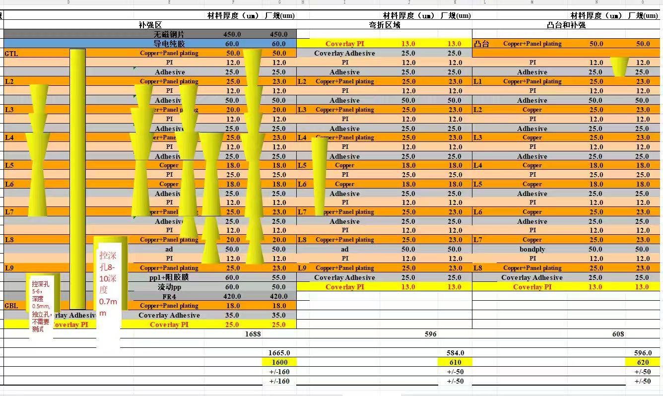
You will see three main types of vias in PCB Via Design. These are through hole, blind, and buried. Each via helps connect layers on printed circuit boards. Look at the table below for their meanings:
Via Type | Definition |
|---|---|
Through-hole | Vias go through the whole board from top to bottom. They connect all layers. |
Blind | Vias connect an outer layer to inner layers. They do not go through the whole board. |
Buried | Vias connect inside layers. They do not reach the outside of the PCB. |
Picking the right via type makes manufacturing easier. It also increases yield rates. Using good design rules helps you avoid defects. Keep aspect ratios low and clearances proper. This makes your PCB more reliable.
Key Takeaways
Learn about the three main types of vias. These are through-hole, blind, and buried. Each type connects layers in a PCB in its own way.
Pick the right via type for your project. Through-hole vias make strong connections. Blind and buried vias save space and help performance.
Use good design rules for vias to make them reliable. Keep aspect ratios low. Make sure there is enough space to stop defects.
Use blind and buried vias for high-speed jobs. They lower signal loss and stop interference. This makes your PCB work better.
Talk to your manufacturer early when you design. This helps your PCB get built well. It also makes sure it meets all needs.
PCB Vias Overview
What Are Vias in PCB?
You will find that vias act as tiny bridges inside a pcb. These small holes let electrical signals or power move from one layer to another. Without vias, you could only route signals on a single layer. This would make your pcb much larger and less powerful. Vias use copper plating to create a path for electricity. You can connect components to inner power planes or link traces across different layers. Vias also help with heat dissipation, which keeps your pcb running smoothly.
Tip: Think of vias as elevators in a tall building. They let signals travel up and down between floors, making sure every part of your pcb works together.
Why Vias Matter in PCB Design
Vias play a key role in pcb design. They make sure all the layers in your pcb can talk to each other. Here are some important reasons why you need vias:
Vias create electrical connections between layers in a multilayer pcb.
They help you build complex circuits in a small space.
Vias improve signal integrity by shortening signal paths and reducing interference.
Proper placement of vias can prevent signal loss and keep your pcb reliable.
Vias support the core operations that make your pcb function as designed.
When you use vias wisely, you boost the performance and reliability of your pcb. You also make it easier to fit more features into a smaller board. Good via choices lead to better results in your projects.
Through Hole Vias
Through Hole Via Definition
Through hole vias are a main type of pcb via hole. These vias start at the top layer and end at the bottom layer. They connect every layer in the pcb. You use them to make strong electrical and mechanical links. Through hole vias are not like blind vias because they go through the whole board.
How Through Hole Vias Work
You make these vias by drilling holes in the pcb. The holes get copper inside so signals can move between layers. Drilling can change how the layers line up. If layers do not match up, your pcb may not work well. Bigger boards can have more problems with alignment. Sometimes tools cannot check the exact spot of the vias. This is why you need to follow good pcb design rules.
Note: Plated through hole connects copper layers. Non-plated through hole gives mechanical support.
Applications of Through Hole Vias
Through hole vias are used in many devices. The table below shows common uses:
Type of Device | Characteristics |
|---|---|
Power Supply Boards | Strong and cheap, not focused on small size |
Industrial Control Systems | Built to last and easy to fix |
Older Consumer Electronics | Use through-hole vias for reliability |
Prototypes | Bigger size makes inspection and fixing easier |
Advantages of Through Hole Vias
Through hole vias give you many good things:
Easy to make and saves money
Strong connection, good for parts under stress
Works well for high power or heat
These vias help your pcb last longer and work well in tough places.
Design Tips for Through Hole Vias
Follow these rules for better results:
Design Rule | Recommendation |
|---|---|
Via Size and Aspect Ratio | Keep aspect ratio under 10:1; for a 1.6mm board, use at least 0.2mm diameter. |
Via Spacing | Keep vias at least 0.5mm apart so the board stays strong. |
Annular Ring Requirements | Make ring at least 0.15mm wide per side; pad should be at least 0.6mm. |
Via Placement Near Components | Do not put vias under surface-mount parts; use tented vias if needed. |
Thermal Via Design | Use 1.0mm to 1.2mm pitch for thermal vias to help heat move. |
Good placement and size choices make your pcb stronger and more reliable. These tips help your pcb handle signals and heat better.
Blind Hole Vias
Blind Hole Via Definition
Blind hole vias are a special type of via in pcb via design. You use these vias to connect an outer layer to one or more inner layers. They do not go all the way through the pcb. This makes them different from through-hole vias, which pass from the top to the bottom. Blind vias help you link surface components to inside layers without making extra holes in every layer.
How Blind Vias Work in PCB
You create blind vias by drilling only partway through the pcb. There are two main ways to make these holes:
Controlled-depth drilling uses a drill that stops at a set depth, so the via does not reach the other side.
Laser drilling happens after all layers are pressed together. A laser burns through the copper and insulation to form the via.
These methods let you connect layers without affecting the whole board. Blind vias are important when you want to save space and keep the pcb compact.
Applications of Blind Vias
You will find blind vias in many high-tech products. They are common in high-density interconnect (HDI) pcb designs. Here are some places where you see them:
Telecommunications equipment, like 5G systems, use blind vias to handle fast signals.
Consumer electronics, such as smartphones and tablets, need these vias for small size.
Medical devices, including portable monitors, use blind vias for compact and reliable circuits.
Automotive systems, like driver-assist units, depend on blind vias for advanced features.
Advantages of Blind Vias
Blind vias give you several benefits over other types of pcb via holes:
They connect outer and inner layers without passing through the whole pcb, which saves space.
You can make smaller boards because blind vias do not block routing on every layer.
In a six-layer pcb, a blind via can link layer 1 to layer 2, leaving layers 3 to 6 untouched. This can shrink the board size by up to 30%.
Blind vias help improve signal quality by shortening the path and reducing unwanted stubs.
Tip: Using blind vias can boost electrical performance and help you fit more features into your pcb design.
Design Tips for Blind Vias
To get the best results with blind vias, follow these tips:
Plan your stackup early to define where you need blind vias.
Give enough annular ring for each layer pair.
Stagger vias to spread out heat and stress.
Mark drilling depths and diameters clearly in your drawings.
Place vias to keep signal paths short and avoid interference.
For high-speed signals, use back-drilling to remove unused stubs.
Check your design with test coupons to make sure the plating and depth are correct.
Talk to your fabricator about their limits for blind via size and build steps.
Blind vias help you create powerful, compact, and reliable pcb designs. You can use them to solve space and signal challenges in modern electronics.
Buried Hole Vias
Buried Via Definition
A buried via connects only the inner layers of a pcb. You will not see this via on the top or bottom. In pcb via design, buried vias make connections inside the board. The outer layers stay open for other traces or parts. A buried via is a plated hole linking two or more inner layers. These holes are hidden from the outside. This feature helps you handle complex multi-layer pcb projects.
How Buried Vias Work in PCB
Buried vias are made early in pcb fabrication. The process has several steps to make sure the vias work well:
Core preparation comes first. Inner layer cores get circuit patterns.
Next is drilling. Mechanical drills make holes in the inner cores.
The holes are copper plated to create a path for electricity.
Epoxy fills the vias to stop air pockets.
The first lamination bonds the inner cores together.
More layers are added in later lamination cycles.
Final processing includes drilling, plating, and finishing the outer layers.
This method keeps buried vias inside the pcb. They do not touch the outer layers. You can use this way to get higher-density routing and better signal quality.
Applications of Buried Vias
Buried vias are used in advanced electronic products. These include:
High-density interconnect pcbs need many connections for complex circuits.
Miniaturized electronics like smartphones, tablets, and wearables.
Medical devices need small and reliable boards.
Buried vias help save space and boost performance in your pcb design.
Advantages of Buried Vias
Buried vias offer many benefits in pcb via design:
You can fit more routes in multilayer pcbs when space is tight.
These vias make signal paths shorter and remove stub effects. This helps your board work faster.
Buried vias free up the surface for more parts and traces.
You get more routing choices, which is good for fine-pitch parts.
You can use fewer routing layers, which may lower costs.
Buried vias help cut down crosstalk and electromagnetic interference. This makes your pcb more reliable.
Tip: Buried vias can improve signal quality and make your board design more flexible.
Design Tips for Buried Vias
When you use buried vias in your pcb, follow good design rules. Put these vias in the inner layers to keep the outer layers clear. This helps keep signals strong and lowers interference. Balance performance, cost, and manufacturability. Always check the smallest drill diameter and biggest aspect ratio for your board. These limits decide how small and deep your holes can be. Plan your layout to use buried vias only where needed. This keeps your pcb strong and cost-effective.
PCB Via Design Comparison
Through Hole vs Blind vs Buried Vias
It is important to know how through hole, blind, and buried vias are different. Each via type has special features. These features change how your pcb works, how much space it uses, and how it is made.
Via Type | Electrical Performance | Space Saving Benefit | Cost Level | Reliability in High-Stress Use |
|---|---|---|---|---|
Through-Hole Vias | Good for power, can lose signal at high speed | Takes more space | Cheapest | Very strong, easy to inspect and repair |
Blind Vias | Shorter paths, less interference, better for high speed | Saves space in high-density designs | More Expensive | Needs careful manufacturing, can crack |
Buried Vias | Shortest paths, best for high speed, less signal loss | Can save up to 50% of surface space | Most Expensive | Reliable if made well, hard to repair |
Through-hole vias use simple drilling. They connect all layers in the pcb. These vias are good for strong links and high-power jobs. Blind vias connect outer layers to inner layers. They do not go through the whole board. This saves space and helps with routing in tight designs. Buried vias connect only inner layers. They let you fit more routes inside the pcb. The surface stays open for parts.
Tip: Blind and buried vias help you make boards that are smaller and faster. They let signals travel shorter distances. This means less delay and better performance.
Blind and buried vias let you:
Fit more routes in a small pcb.
Make thermal and electrical performance better by shortening layer distances.
Cut down signal interference and delays, which is important for fast circuits.
Keep the outer layers open for more parts and traces.
But you also need to think about cost and manufacturability. Through-hole vias cost the least because they use simple drilling. Blind vias cost more since they need special drilling methods. Buried vias cost the most because they need complex steps and careful stacking.
Via Type | Cost Level | Manufacturing Process Description |
|---|---|---|
Through-Hole Vias | Cheapest | Simple mechanical drilling, easy to implement, larger space requirement. |
Blind Vias | More Expensive | Requires special methods like laser or depth drilling, connects outer layers to inner ones. |
Buried Vias | Most Expensive | Involves sequential lamination, complex and time-consuming, ideal for compact designs. |
Reliability matters too. Through-hole vias are strong and reliable. They work well for parts under stress. Blind vias can make signals better but may crack if not made right. Buried vias work well in multilayer pcbs. Their hidden spot makes repairs harder.
Choosing the Right Via for Your PCB
Pick the via type that matches your project needs. Think about what your pcb must do and what limits you have.
If you want low cost and strong links, use through-hole vias. They are best for power boards, prototypes, and boards where space is not tight.
If you need to save space and boost performance, use blind vias. Blind vias are great for high-density designs like smartphones and advanced electronics. They help you route signals in tight spaces and keep the board small.
If your design is very complex and needs many routes inside, pick buried vias. Buried vias let you save up to 50% of surface space and use your pcb layers well.
Always check manufacturability rules before you pick a via type. Dfm means designing so your pcb can be built easily. Each via type has its own manufacturability rules. Through-hole vias are simple, but blind and buried vias need more planning. Talk to your manufacturer about their limits for drilling, aspect ratio, and layer stacking.
Note: If you work with high-frequency signals, blind and buried vias help keep signal quality high and reduce signal loss. Microvias are also good for very fine and fast designs.
Think about repair and inspection too. Through-hole vias are easy to check and fix. Blind and buried vias are harder to inspect. You must follow all manufacturability rules to avoid problems.
In summary, balance your needs for cost, space, performance, and reliability. Pick the via type that fits your pcb via design best. Always follow manufacturability rules and talk to your fabricator early. This helps you get a pcb that works well and meets your needs.
You can find out how each via type is different and used by looking at the table below:
Via Type | Cost Level | Difficulty to Make | Best Use Cases |
|---|---|---|---|
Through-Hole | Low | Easy | Older designs needing strong connections and heat control |
Blind | Medium | Medium | High-frequency designs like smartphones and graphics cards |
Buried | High | Hard | Compact, high-performance multi-layer pcbs in automotive, medical |
If you know about these via types, you can:
Make electrical performance better
Make your pcb stronger
Help your pcb get made faster
Picking the right via lets you build a pcb that works well for your project.
FAQ
What is the main difference between through-hole, blind, and buried vias?
You use through-hole vias to connect all layers. Blind vias link an outer layer to inner layers. Buried vias connect only inner layers. Each type helps you route signals in different ways.
Can you repair a blind or buried via if it fails?
Repairing blind or buried vias is hard. You cannot reach them easily. Through-hole vias are easier to fix. You should follow good design rules to avoid problems.
Why do high-speed PCBs use blind and buried vias?
High-speed PCBs need short signal paths. Blind and buried vias reduce signal loss and interference. You get better performance and smaller boards with these vias.
How do you choose the right via for your PCB project?
You look at your board’s size, cost, and performance needs. Through-hole vias work for simple boards. Blind and buried vias fit compact, high-speed designs. Ask your manufacturer about their limits.
See Also
Understanding Blind, Buried, and Through-Hole Vias Differences
Exploring Buried Vias in Multilayer PCBs and Solutions
Optimizing Space and Performance with Blind Vias Technology
