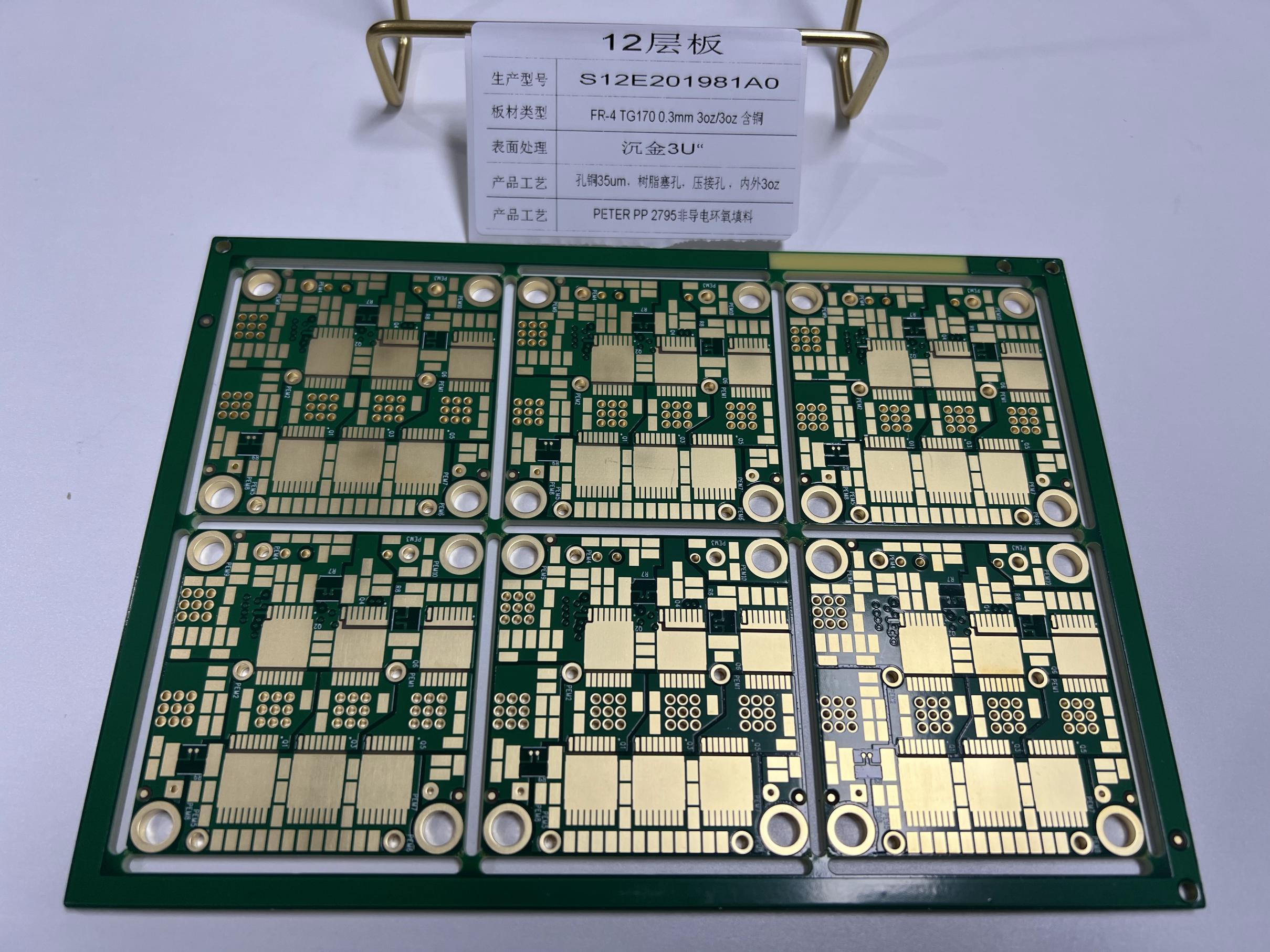
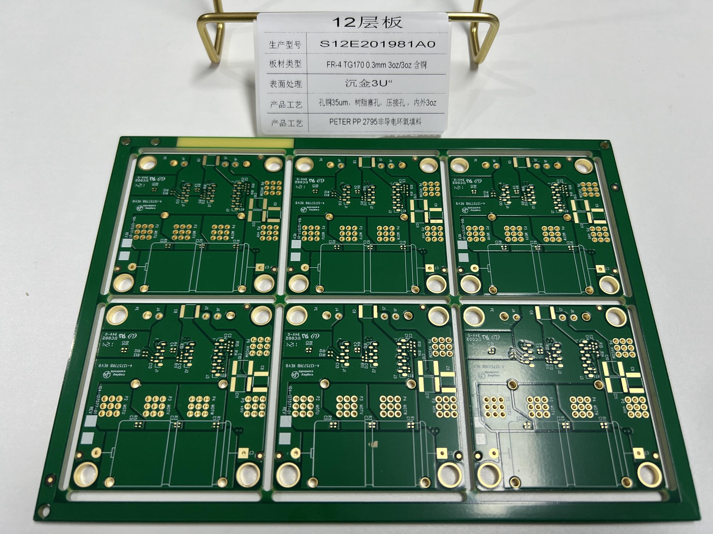
Production Technology Guide for heavy Copper Multilayer PCBS

Heavy copper circuit boards are utilized for their strong power and reliability. They carry high currents and manage heat exceptionally well. New production technology guides have led to methods that enhance the performance of these boards while reducing costs. For instance, these advancements have resulted in a 10% reduction in material waste, a 40% decrease in energy consumption, and a 20% cut in costs. This guide illustrates how innovative ideas contribute to the creation of tough and dependable boards.
Key Takeaways
Heavy copper PCBs are important for devices needing lots of power. They handle heat well and carry strong currents, working reliably in hard conditions.
Picking the right copper thickness is very important. Thicker copper layers spread heat better and carry more current, improving how the PCB works.
Good ways to manage heat, like thermal vias and heat sinks, are key. They help move heat around and stop devices from getting too hot.
Key Design Considerations for Heavy Copper PCBs
Copper Thickness and Its Role in Performance
Copper thickness is very important for heavy copper PCBs. Thicker copper helps spread heat better, stopping hotspots from forming. This is crucial for high-power devices where too much heat can harm parts. Thicker copper also carries more current, preventing overheating and energy waste.
Aspect | Benefit |
|---|---|
Heat Dissipation | Spreads heat evenly to avoid damage. |
Current Carrying Capacity | Handles high currents without overheating or wasting energy. |
Mechanical Strength | Makes the PCB stronger against bending or twisting. |
Longevity | Lasts longer through repeated heating and cooling cycles. |
Choosing the right copper thickness ensures the PCB works well in tough conditions. Heavy copper PCBs usually have 3 or more ounces of copper per layer. This improves their ability to handle heat and electricity.
Managing Layer Count and Complexity
The number of layers in a PCB affects how easy it is to make and how well it works. More layers can cause problems like misaligned inner layers or gaps in resin. These issues weaken the PCB's structure.
Resin gaps or delamination |
Misaligned inner layers |
Over-etching during production |
Trouble adjusting etch factors |
To avoid these problems, work closely with your PCB maker. Simplify the design and ensure layers align properly during production. This makes the PCB stronger and lowers production costs.
Thermal Management in Heavy Copper PCBs
Good thermal management is key for heavy copper PCBs, especially in high-power devices. Copper placement, thermal vias, and heat sinks help spread heat. Placing parts carefully ensures heat spreads evenly. Thick copper traces reduce power loss.
Heavy copper lets PCBs carry more current without needing wider traces. This boosts efficiency and heat control. Testing materials for thermal conductivity during design helps improve heat management.
Electrical Performance and Signal Integrity
Strong electrical performance is vital for heavy copper PCBs. These PCBs are tested to meet standards for signal quality and current flow. Testing ensures the design matches the electrical needs.
Heavy copper PCBs are great for high-power uses. They carry more current, manage heat well, and are physically strong. They work reliably in tough environments. Fewer layers for power distribution mean smaller designs, which is useful for modern electronics.
Step-by-Step Production Technology Guide for Heavy Copper Multilayer PCBs

Material Selection and Layer Preparation
Picking the right materials is key for strong heavy copper PCBs. Use high-quality bases like FR-4 or polyimide. These materials handle heat well. For thicker copper, choose materials that spread heat better.
Preparing layers means cleaning and treating the base material. This helps copper stick properly and avoids defects. Good preparation also stops layers from peeling during production.
Etching Techniques for Heavy Copper
Etching creates the copper patterns on the PCB. Advanced etching methods are needed for thick copper layers. Chemical etching works well, but special tools may be required for prototypes.
Watch the etching process carefully to avoid over-etching. Adjust settings based on copper thickness and design complexity. This keeps copper traces clean and ensures good electrical performance.
Lamination and Bonding Processes
Lamination joins copper layers to make the PCB. Heat and pressure are used to bond them tightly. Strong bonds improve the device's stability and reliability.
🛠️ Tip: Plan for heat stress during lamination. Sudden temperature changes can weaken copper bonds. Use quality materials and adjust bonding conditions to prevent this.
Drilling and Hole Formation
Drilling makes holes to connect copper layers. Laser drilling is fast and precise for small holes. Mechanical drills work better for larger holes.
New drilling tools improve hole quality and speed. For example, dual-beam lasers can drill 1000 holes per second. This makes them great for heavy copper PCBs.
Plating and Step Plating for Thick Copper Layers
Plating adds more copper to the PCB. Step plating builds copper thickness layer by layer. This keeps copper even and avoids problems like gaps.
Electroplating is common for this step. Control the process carefully to get the right thickness without weakening the PCB.
Final Testing and Quality Assurance
Testing is the last step to ensure the PCB works well. Functional Circuit Testing (FCT) checks how the board performs in real conditions. Keeping inspection records helps with audits and standards.
✅ Note: Use traceability systems to track each PCB. This ensures quality and helps meet industry rules. Records also help with future checks.
High-quality production ensures heavy copper PCBs work reliably in tough situations.
Benefits and Applications of Heavy Copper PCBs
Industries That Use Heavy Copper PCBs
Heavy copper PCBs are important in many industries. They handle high power and tough conditions. These industries depend on their strength and performance:
Telecommunications: They help 5G networks send data fast and keep signals clear.
Renewable Energy: They make solar inverters and wind controllers work well in bad weather.
IoT and Smart Devices: IoT gadgets need them for better power use and data handling.
Sector | Growth Rate (CAGR) | Key Uses |
|---|---|---|
Automotive | Over 10% | Electric cars, power systems |
Telecommunications | High-speed circuits | |
Renewable Energy | High demand | Solar systems, energy controllers |
Industrial | Increasing need | Robots, smart factories |
Strong and Reliable Design
Heavy copper PCBs are tested to ensure they last long. The Peel Strength Test checks how well layers stick together. This stops layers from coming apart under heat or pressure. Their tough build makes them perfect for high-power uses in hard conditions.
Great Heat and Power Handling
These PCBs are excellent at managing heat and electricity. They spread heat well, stopping parts from overheating. Tests like thermal stability at peak power and maximum current load capacity prove they work under stress.
Metric | What It Measures |
|---|---|
Maximum current load capacity | Checks the highest current the PCB can handle safely. |
Thermal stability at peak power | Tests if the PCB works well under high heat. |
Heat transfer rate | Shows how quickly heat moves from parts to the copper. |
Resistance across traces | Measures how much power is lost in the copper paths. |
Built for High Power Needs
Heavy copper PCBs are made for devices needing lots of power. Thick copper layers let them carry more current without getting too hot. Tests ensure they handle power safely. This makes them key for industries like cars and renewable energy systems.
Quality Control and Reliability Testing in Heavy Copper PCB Production

Visual Checks for Surface Problems
Visual checks help find surface problems on heavy copper PCBs. Issues like uneven coatings or discoloration can be spotted early. Tools like X-ray fluorescence (XRF) and infrared tests make detection better. For example, XRF tests check ENIG surfaces for black pad oxidation or nickel exposure. HASL coatings are tested for uneven tin using heat analysis.
Surface Type | Common Problems | How to Detect |
|---|---|---|
ENIG | Black pad, Nickel exposure | XRF test, 200x cross-section |
HASL | Tin icicles, Dewetting | Heat profile, Solderability test |
OSP | Discoloration, Film peeling | IR test, Tape adhesion test |
Digital systems record these checks instantly. This helps fix problems fast and lowers defect rates.
Stress Tests for Toughness
Stress tests check if PCBs can handle tough conditions. They simulate heat, pressure, and repeated temperature changes. Peel strength tests measure how well copper layers stick under stress. These tests find weak spots early and make designs stronger.
Electrical Tests for Good Performance
Electrical tests ensure PCBs work as expected. Continuity tests check if all connections are complete. Isolation tests look for unwanted shorts. Flying probe tests are great for prototypes and small batches. Bed-of-nails tests work well for large production runs.
Test Type | Purpose | Features |
|---|---|---|
Continuity Testing | Measures resistance levels. | |
Isolation Testing | Finds unwanted shorts. | Ensures nets stay separate. |
Flying Probe Testing | Good for prototypes. | Flexible and precise. |
Bed of Nails Testing | Best for big production runs. | Tests many points at once. |
These tests make sure PCBs perform well, even under high power.
Following Industry Rules
Meeting industry rules is important for PCB production. Audits check if standards like IPC-6012C for copper thickness are followed. IPC-A-600G ensures PCBs look good, and ISO 9001:2015 confirms quality systems are strong.
Standard | What It Covers | Pass Rate |
|---|---|---|
IPC-6012C | Copper thickness, hole quality. | |
IPC-A-600G | Visual quality of PCBs. | >99% |
ISO 9001:2015 | Quality management systems. | N/A |
Following these rules ensures PCBs meet global standards and work reliably.
Practical Tips for Making Heavy Copper PCBs with LT CIRCUIT
Avoiding Common Manufacturing Problems
Making heavy copper PCBs can have issues like damage or mistakes. These problems often happen because of poor design choices. Fixing designs can lower costs and reduce waste a lot.
Metric | Before Fixing | After Fixing |
|---|---|---|
Lot Reject Rate (LRR) | 900 PPM | |
Fault Rate | 0.76% | Lowered |
To prevent these problems:
Align layers correctly during lamination.
Use better etching methods to avoid over-etching.
Work with skilled makers like LT CIRCUIT to improve designs.
Tip: Keep your PCB design simple to make it easier to produce.
Eco-Friendly Practices in PCB Production
Being eco-friendly is important in PCB making. You can help the planet and still make great PCBs.
Use recycled copper to save energy and reduce mining.
Follow RoHS and REACH rules to use safe materials.
Try biodegradable materials to cut down on waste.
Use lead-free solder for greener production.
Eco-friendly steps help the environment and meet global rules. For example, recycling copper saves energy and reduces harm to nature.
Working with LT CIRCUIT for Great Results
LT CIRCUIT provides advanced tools for making heavy copper PCBs. They focus on quality and use the latest technology. Industries like space and electric cars have improved by working with them.
Industry/Application | Improvement/Result | Impact/Stat |
|---|---|---|
Aerospace Applications | 30% smaller PCBs, making satellites lighter | Cheaper launches and more features |
Electric Vehicles (EVs) | 10% cooler control units | Longer-lasting and better-performing vehicles |
Choosing LT CIRCUIT means you get expert help to make top-quality PCBs.
Saving Money Without Losing Quality
You can cut costs and still make great PCBs with smart planning. Here’s how:
Pick common parts to get better prices.
Test designs with small batches before making more.
Combine small orders into bigger ones to save money.
Add test points to make testing easier and faster.
Note: Use machines for simple tasks and people for tricky ones. Mixing both saves money and time.
By using these tips, you can save money and still make strong, reliable heavy copper PCBs.
Advanced production methods help heavy copper PCBs work well in tough conditions. Good design and manufacturing bring important advantages:
Increased Durability: Strong copper layers handle stress better.
Higher Conductivity: Even copper layers improve signal quality.
Environmental Impact: Eco-friendly steps cut down on waste.
Working with LT CIRCUIT ensures top quality, new ideas, and great results for your PCB projects.
FAQ
What does extreme copper do in multilayer PCBs?
Extreme copper helps carry more current and manage heat. It makes the PCB stronger and more reliable for high-power uses.
How does heavy copper design improve heat control?
Heavy copper design spreads heat better across the PCB. This stops overheating and keeps the PCB working well in tough conditions.
Why is picking the right material important for multilayer PCBs?
The material affects how strong and heat-resistant the PCB is. Good materials help the PCB last longer and work in harsh environments.
See Also
Understanding The Production Steps For Rigid-Flex Circuit Boards
Utilizing Horizontal Copper Sinking Technology In PCB Manufacturing
Challenges And Processes In Multi-Layer Circuit Board Prototyping
Key Guidelines For Designing High Current Heavy Copper PCBs
Essential Knowledge For Multi-Layer PCB Layout Design Mastery

