How a Professional PCB Manufacturer Handles Multilayer and High-Density Interconnect Boards
A Professional PCB Manufacturer like LT CIRCUIT uses new technology and strong quality checks to make multilayer and high-density interconnect boards. LT CIRCUIT uses laser drilling that is very exact, automated optical inspection, and trained workers. This helps make sure every board is reliable and works well. Every board meets the rules for the industry.
Key Takeaways
LT CIRCUIT uses new technology like laser drilling and automatic checks to make strong multilayer and HDI PCBs. These boards can hold more circuits in smaller spaces.
Careful planning, picking the right materials, and exact steps help LT CIRCUIT make tough, high-quality boards. These boards work well in phones, medical tools, and airplanes.
Careful quality checks with AI and real-time tests make sure every board is good. Each board meets industry rules and works well in hard situations.
Multilayer and HDI PCB Basics
Definitions
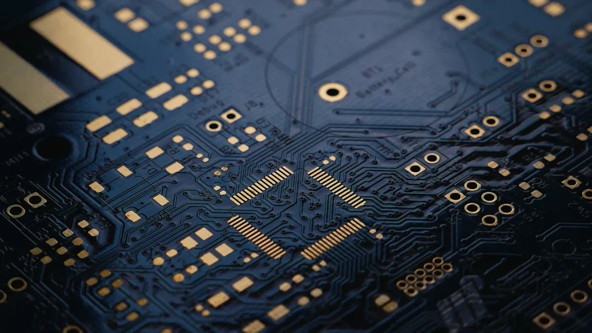
Multilayer PCBs have three or more layers of metal. These layers are stacked and pressed together. This lets the boards fit more circuits in a small space. LT CIRCUIT makes multilayer PCBs with up to 20 layers. These boards help advanced electronics work better. High-Density Interconnect PCBs use special methods like microvias and laser drilling. These boards can fit more connections in tiny spaces. LT CIRCUIT’s HDI PCBs have stackup choices like 1+N+1 or 2+N+2. This makes them great for small, powerful devices.
Metric/Feature | HDI PCBs | Standard Multilayer PCBs |
|---|---|---|
Routing density on inner layers | Baseline | |
Number of layers | Typically fewer (e.g., 6 layers replacing 8 layers) | Higher (e.g., 8 layers) |
Component density (parts per unit area) | Higher | Lower |
Via technology | Blind, buried, microvias; laser drilling | Through-hole; mechanical drilling |
Maximum layers possible | Over 20 layers | Generally fewer layers |
Signal integrity | Improved | Lower |
Board size and weight | Smaller, lighter | Larger, heavier |
Features and Uses
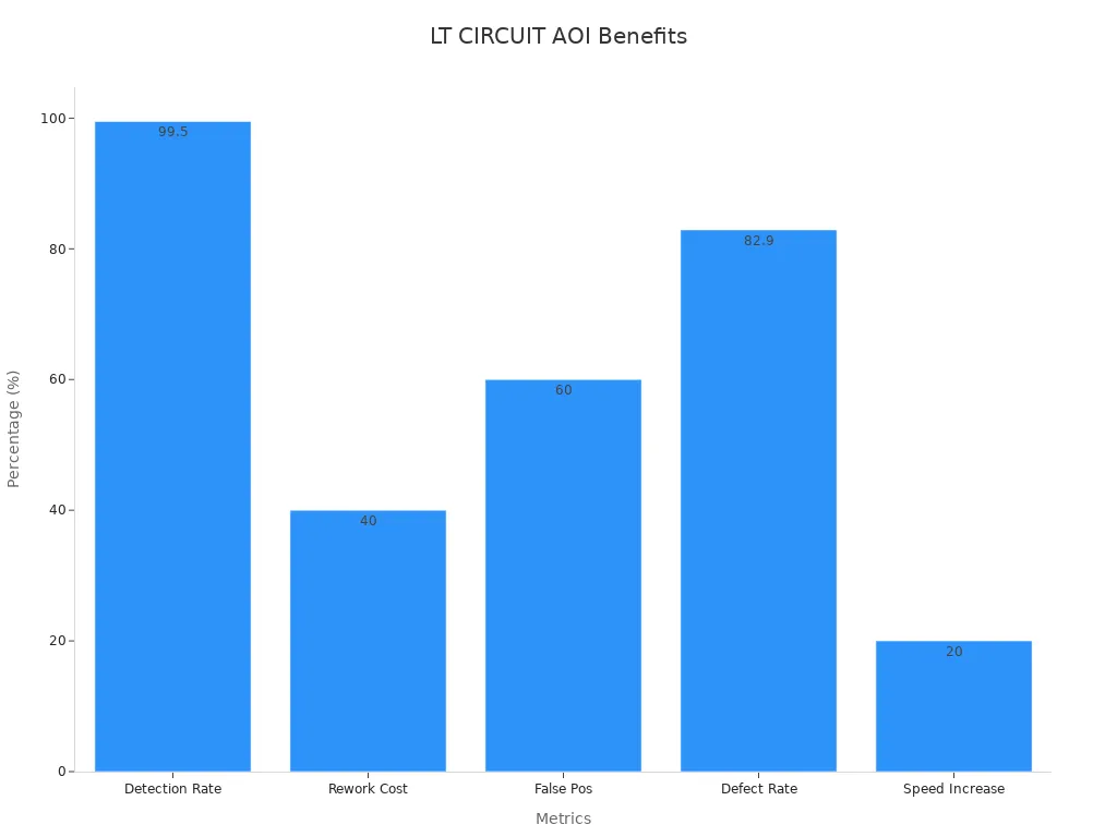
Multilayer and HDI PCBs have many good points. They let you put more parts on the board. They keep signals clear and make boards smaller. LT CIRCUIT uses strong materials and careful steps to stop water from getting in. This also stops copper from moving where it should not. These things help the boards last longer, even in hard places. LT CIRCUIT uses machines to check for problems. These machines find almost all defects, much more than people can. This also makes boards faster to build and cheaper to make.
Engineers use these boards in phones, medical tools, and planes. HDI PCBs work with lots of pins and tiny parts. This makes them needed for new electronics. LT CIRCUIT makes sure every board is safe and works well in every job.
Professional PCB Manufacturer Process
Design and Engineering
A Professional PCB Manufacturer starts with careful planning. LT CIRCUIT uses special software and skilled workers to design each board. They decide how many layers the board needs. They also choose how to stack the layers and where to put power and ground planes. These choices help the board send signals clearly and stay strong.
LT CIRCUIT follows important rules like IPC/JPCA-2315 and IPC-2226. These rules help design high-density interconnects and microvias. Engineers also use IPC/JPCA-4104 and IPC-6012 to pick materials and check quality.
Benchmark Category | Key Metrics / Practices | Impact on Performance and Efficiency |
|---|---|---|
Layer Stack-Up Design | Number, sequence, and symmetry of layers; spacing between layers; dedicated power and ground planes | Enhances signal integrity, power distribution, EMI reduction, and mechanical stability |
Material Selection | Dielectric constant (Dk), loss tangent (Df), thermal conductivity, coefficient of thermal expansion (CTE) | Improves signal speed, reduces signal loss, ensures thermal management and reliability |
Via Design and Placement | Use of through-hole, blind, buried, and microvias; minimizing via inductance; via-in-pad; thermal vias | Optimizes signal integrity, routing density, and thermal dissipation |
Power Distribution & Ground | Dedicated power and ground planes; minimizing return paths | Reduces noise, voltage fluctuations, and improves power integrity |
Design Efficiency Practices | Optimized component placement, trace routing, power distribution, signal integrity management, thermal management | Enhances overall circuit performance and reliability |
Testing & Standards | Adherence to IPC/JPCA standards (IPC/JPCA-2315, IPC-2226, IPC/JPCA-4104, IPC-6012); signal integrity, thermal, EMI/EMC testing | Ensures quality, reliability, and compliance with industry benchmarks |
A Professional PCB Manufacturer like LT CIRCUIT uses these steps to make sure boards work well everywhere.
Material Selection
Picking the right material is very important. LT CIRCUIT chooses materials for speed, low loss, and strength. They use FR-4 for most boards. For faster boards, they use Isola I-Speed or I-Tera MT40. These materials help signals move quickly and stay clear.
PCB Material Category | Key Properties and Reliability Factors | Typical Applications and Examples |
|---|---|---|
Normal speed and loss | Higher dielectric constant variation with frequency, higher dielectric loss, typical FR-4 materials | Suitable for low GHz digital/analog; e.g., Isola 370HR |
Medium speed and loss | Flatter dielectric constant vs frequency, about half the dielectric loss of normal speed materials | Suitable up to ~10 GHz; e.g., Nelco N7000-2 HT |
High speed and low loss | Flatter dielectric constant response, low dielectric loss, reduced electrical noise | Suitable for high-speed digital; e.g., Isola I-Speed |
Very high speed and very low loss (RF/microwave) | Flattest dielectric constant response, minimal dielectric loss | Suitable up to ~20 GHz RF/microwave; e.g., Isola I-Tera MT40, Tachyon 100G |
LT CIRCUIT checks every supplier and controls the process. They look at things like thermal conductivity and dielectric constant. These checks help the board last longer and work better.
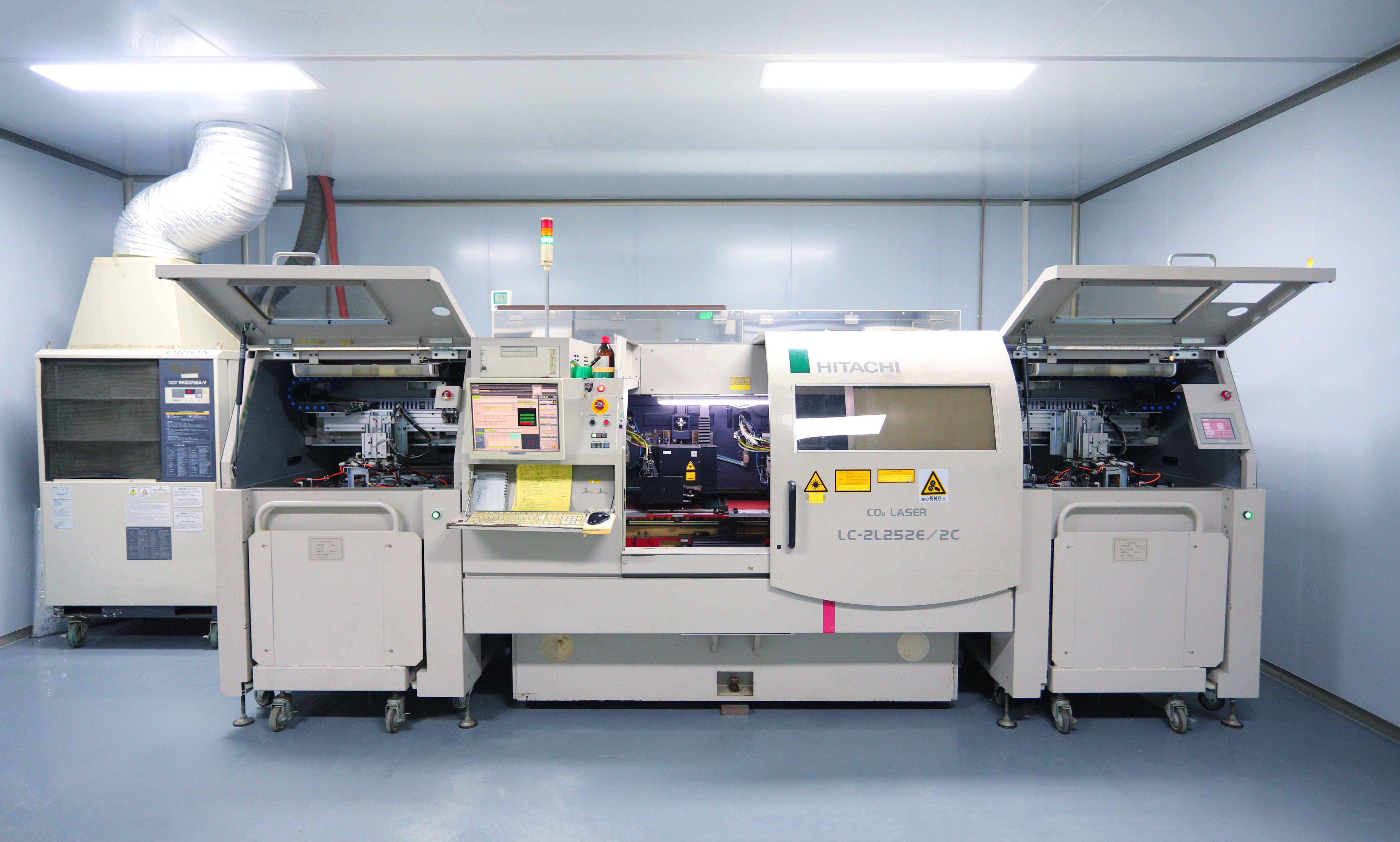
Lamination and Drilling
Lamination and drilling come next. LT CIRCUIT stacks copper, inner cores, and prepreg carefully. They use targets to line up each layer. Heat and pressure glue the layers together. This makes the board strong and ready for holes.
Drilling uses lasers and machines. Lasers can make up to 1,000 holes each second. CO2 lasers drill holes as small as 30-40 microns. UV lasers can go down to 20 microns. Machines spin fast and can drill holes as small as 50 microns. LT CIRCUIT keeps holes in the right place within 10 microns. Copper in the holes stays even at 15-20 microns thick. Hole resistance stays below 1,000 micro-ohms.
Process Aspect | Numerical Evidence / Specification |
|---|---|
Laser drilling speed | Up to 1000 holes per second (10x increase from initial machines) |
CO2 laser aperture limit | 30-40 microns |
UV laser aperture range | 20-50 microns (predicted expansion after 2022) |
Mechanical spindle speed | Ultra-high speed spindles reaching 250,000 rpm |
Mechanical drilling aperture | Achievable down to 50-70 microns with ultra-high speed spindles |
Hole positioning accuracy | Within a few microns to 10 microns |
Copper layer thickness in holes | Uniform 15-20 microns thickness |
Hole resistance | Below 1000 micro-ohms |
Via Technology
Via technology helps connect the layers. LT CIRCUIT uses microvias, blind vias, and buried vias. These vias let engineers fit more parts in a small space. Filling and plating vias make connections stronger. This also helps stop electromagnetic interference.
HDI PCBs let you fit more lines and smaller spaces.
Filling and plating vias make boards work better and last longer.
Via filling plating makes plugging and connecting faster and more exact.
Hole filling electroplating stops problems and makes boards better.
These ways are important for things like phones and laptops.
Performance Measure | Quantitative Metric / Description |
|---|---|
Maximum Layers in Multilayer PCB | |
Routing Density Increase | 15-20% increase per additional layer |
Component Density in HDI PCB | Exceeds 400% increase |
Impedance Tolerance | Within ±5% |
Electromagnetic Interference (EMI) Reduction | 25-40 dB reduction |
Via Aspect Ratio Improvement | From 12:1 (standard) to 6:1 (HDI via laser drilling) for reliability |
Thermal Conductivity | Copper planes with 385 W/m·K for heat dissipation |
Routing Efficiency Improvement | 35% improvement via AI-driven placement algorithms |
Manufacturing Issue Detection | 95% of potential issues identified by automated DRC tools |
Timing Closure Improvement | 40-60% improvement with machine learning routing optimization |
Quality Control
Quality control is the last step. LT CIRCUIT uses special tools to watch for problems and fix them. Automated Optical Inspection finds missing or wrong parts. X-ray checks for hidden problems under parts. Tests make sure each board works in real life.
LT CIRCUIT uses test coupons and vehicles to check for problems and strength.
Fast tests like thermal cycling and stress tests show if the board is strong.
All tests follow IPC rules, so results are trusted.
Daisy-chain test vehicles help check HDI PCB strength under stress.
LT CIRCUIT also uses real-time checks and AI to find problems. These tools catch 95% of issues and help keep work fast and correct. Their system gives reports to help improve all the time.
A Professional PCB Manufacturer like LT CIRCUIT uses smart planning, careful building, and strong checks. This makes sure every multilayer and HDI PCB is high quality and works well.
A professional PCB manufacturer like LT CIRCUIT makes strong and dependable multilayer and HDI PCBs.
New 5G PCBs need very thin lines and special ways to handle heat.
Any-Layer HDI and built-in parts help make boards smaller and more reliable.
LT CIRCUIT’s skill helps build tough and efficient boards for hard projects.
FAQ
What makes HDI PCBs different from standard multilayer PCBs?
HDI PCBs use microvias and laser drilling. These let more connections fit in small spaces. Standard multilayer PCBs use bigger vias and mechanical drilling.
How does LT CIRCUIT ensure PCB quality?
LT CIRCUIT uses machines to check boards with cameras and X-rays. They also test boards while making them. Skilled engineers watch every step. This makes sure each board follows strict rules.
Can LT CIRCUIT handle custom PCB requirements?
LT CIRCUIT can make boards with special layers, materials, and finishes.
Engineers talk with clients to meet their needs.
The team helps with special tests and design ideas.
See Also
Challenges And Steps In Producing Multi-Layer Circuit Boards
Essential Design Factors For Reliable HDI PCB Production
How Multilayer Rigid-Flex Circuit Boards Are Manufactured
Comprehensive Guide To Heavy Copper Multilayer PCB Technology
Step-By-Step Overview Of Multilayer PCB Manufacturing Process