Advanced Capabilities of Professional PCB Manufacturers for High-Performance Applications
Electronic systems are getting smaller and more complex. In aerospace and automotive fields, tiny devices like CubeSats use special materials. They also need high-density interconnects and careful manufacturing.
Aspect | Details |
|---|---|
Market Valuation 2024 | |
Projected CAGR (2025-2032) | 9.2% |
Key Drivers | Small, energy-saving devices; 5G, IoT, automotive |
Professional PCB manufacturers give the accuracy, trust, and new ideas needed for these high-performance uses.
Key Takeaways
Professional PCB manufacturers use careful methods and special materials. They make small, strong, and fast circuit boards. These boards must meet high quality rules.
Embedded parts and smart ways to put boards together save space. They also help signals work better. This makes PCBs good for hard and quick electronic devices.
Careful testing and certifications make sure each PCB works in hard places. This helps customers trust products for planes, hospitals, and cars.
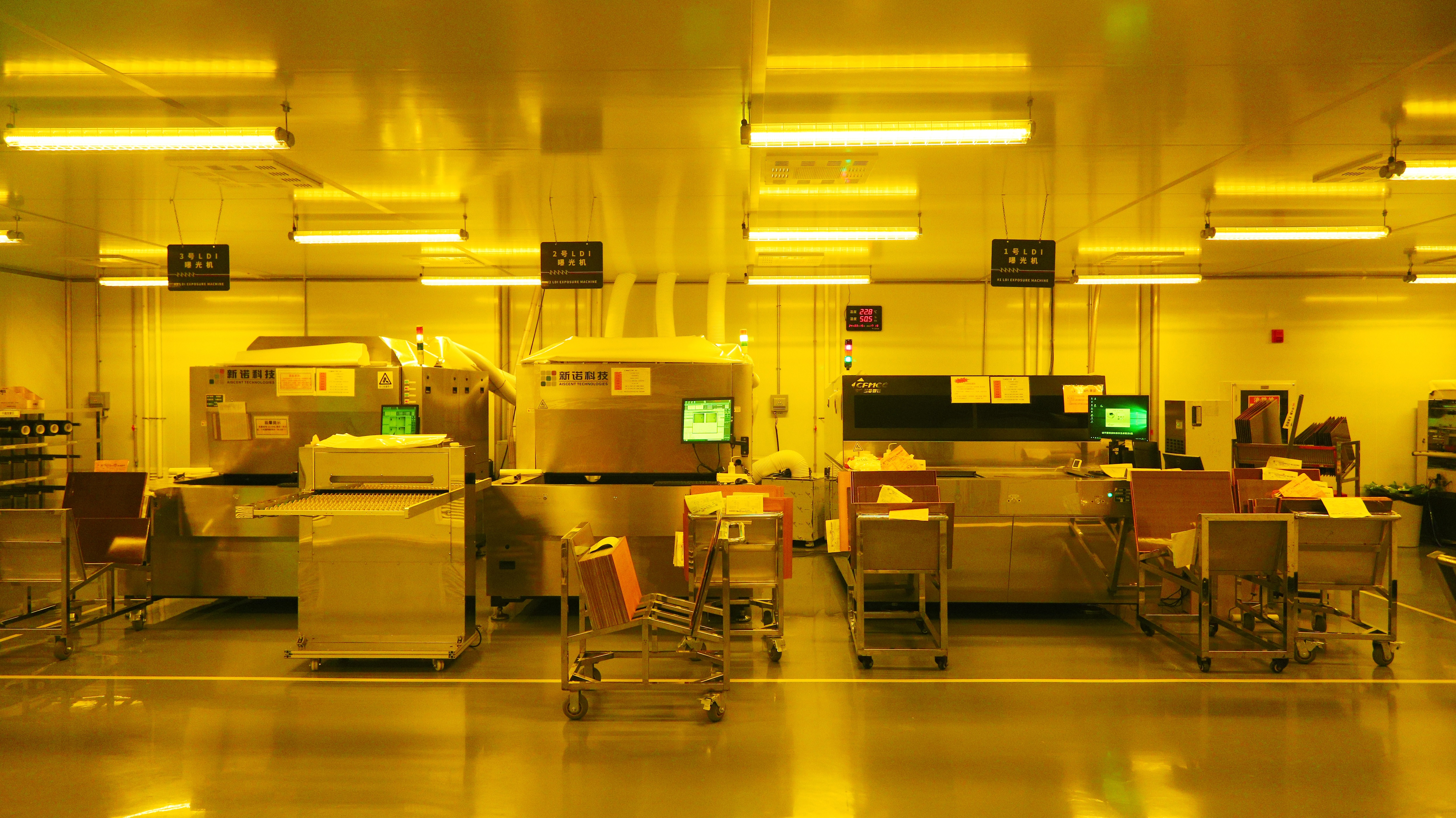
Precision Manufacturing
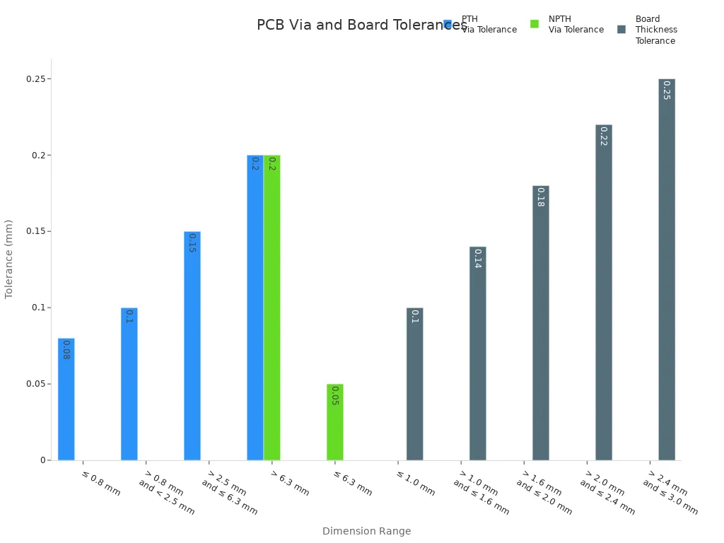
Fine Lines & Small Vias
Professional PCB manufacturers can make very thin lines and small vias. They use special machines and follow strict rules to do this work. These rules help them keep everything the right size. Every trace and via must match the design exactly. This is important for circuits that work very fast or use high frequencies.
Via Type | Via Diameter Range | Typical Manufacturing Tolerance |
|---|---|---|
Plated Thru-hole (PTH) | ≤ 0.8 mm | ± 0.08 mm |
> 0.8 mm and < 2.5 mm | ± 0.1 mm | |
> 2.5 mm and ≤ 6.3 mm | ± 0.15 mm | |
> 6.3 mm | ± 0.2 mm | |
Non-Plated Thru-hole (NPTH) | ≤ 6.3 mm | ± 0.05 mm |
> 6.3 mm | ± 0.2 mm |
Board Dimension | Range | Tolerance |
|---|---|---|
Board Thickness (Finished) | ≤ 1.0 mm | ± 0.10 mm |
> 1.0 mm and ≤ 1.6 mm | ± 0.14 mm | |
> 1.6 mm and ≤ 2.0 mm | ± 0.18 mm | |
> 2.0 mm and ≤ 2.4 mm | ± 0.22 mm | |
> 2.4 mm and ≤ 3.0 mm | ± 0.25 mm | |
> 3.0 mm | ± 10% | |
Board Size (Finished) | N/A | ± 0.1 mm to ± 0.3 mm |
Manufacturers follow IPC standards like IPC-2221 and IPC-2222. These rules tell them the smallest trace widths, via sizes, and spacing they can use. Some boards need trace widths as small as 5 mils. Via drill sizes can be as tiny as 8 mils. Microvias in HDI designs can be 6 mils or even smaller. Laser drilling and careful plating help make these small features.
Keeping everything the right size helps signals stay strong. If traces and vias are not right, signals can get weak or noisy. Good signal quality is needed for advanced electronics to work well.
High-Density Interconnects
High-density interconnect technology lets more parts fit in a small space. Manufacturers use microvias, thin traces, and many layers to build these boards. HDI PCBs have shorter traces, which helps stop noise and keeps signals clear.
HDI boards use microvias and blind or buried vias to save space.
Thin traces and close spacing allow more complex circuits.
Stacking layers and smart design help stop interference and crosstalk.
Laser drilling makes microvias with smooth walls. This helps make more connections and keeps signals strong. Making the aspect ratio of microvias just right makes them stronger and keeps impedance steady. These things make HDI PCBs great for fast, high-frequency, and tiny devices.
Advanced Materials

High-Performance Laminates
High-performance laminates are very important in making advanced PCBs. These materials, like CF-004, polyimide, and Rogers laminates, have special features that regular FR-4 does not have. CF-004 is good because it has strong dielectric strength, stays stable with heat, and has a low dissipation factor. These things help stop signal loss and keep the board steady in tough places. Polyimide substrates can handle very hot or cold temperatures and strong chemicals. This makes them great for aerospace and military electronics. Rogers laminates have low dielectric loss and move heat well. This helps them work well in RF and microwave circuits.
Material Type | Key Properties | Examples / Notes |
|---|---|---|
Low dielectric constant, low dissipation factor, thermal stability, minimal signal loss | Rogers RO4000, Taconic CERFREE, PTFE, LCP, Isola FR-408 | |
Specialized Materials | High dielectric strength, thermal stability, low dissipation factor, mechanical robustness | CF-004 (used in high-frequency, RF circuits, multilayer PCBs) |
These special laminates keep electrical properties steady at high frequencies. They also help control heat and make the board stronger. This is very important for 5G, radar, and car systems.
Metal-Core & Flexible Boards
Metal-core and flexible PCBs are used in industries that need very reliable boards. Metal-core PCBs have a metal base, usually aluminum or copper, that helps move heat away fast. This design helps the board stay cool and last longer. These boards are also strong and keep their shape, so they work well in rough places.
Metal-core PCBs are used in LED lights, power supplies, car electronics, and planes.
The metal layer helps heat move out and supports parts that use a lot of power.
These boards can handle shaking and stress, which is important for medical and factory equipment.
Flexible PCBs use materials like LCP and polyimide. They can bend without breaking or losing how well they work. This lets designers make small, light devices for wearables, medical sensors, and foldable electronics.
Embedded Components
Today, PCB manufacturers can put parts inside the board layers. This helps save space and makes the board work better for fast and crowded circuits. Engineers use special ways like embedded die packaging and mixing different chips on one board. AI design tools help find the best spots for these parts. This keeps signals strong and helps with heat. These new ideas help cars, planes, and 5G systems.
Buried Capacitors
Buried capacitors have a thin layer between power and ground inside the PCB. This layer holds energy with very little inductance. That is important for steady power at high speeds. Putting capacitance inside the board cuts down noise and stops voltage changes. It also gives more room on top for other parts. This lets devices be smaller and hold more parts.
Buried capacitance layers make easy paths for power.
These layers help with good Power Distribution Network design.
Wearable health trackers and car safety systems work better with these layers.
Note: Buried capacitors help make small, strong electronics for today’s needs.
Buried Resistors
Buried resistors are inside the board, close to signal lines. This makes signal paths shorter and cuts down on noise. Engineers pick steady materials like NiCr or TaN thin films for exact resistance.
Picking the right material keeps resistors steady and accurate.
The board design puts resistors near important signals for better signal strength.
Simulation tools check impedance and crosstalk before making the board.
Makers must be careful so they do not hurt the resistors during building.
Buried resistors lower unwanted effects, help match impedance, and give more space on top. These things let more parts fit and make the board work better, especially for fast and trusted electronics.
Assembly Capabilities
Auto-Calibrated SMT
Professional PCB makers use auto-calibrated SMT for accurate part placement. These machines check their vision tools often. They also adjust for nozzle wear to keep errors low. This can lower mistakes by up to 20%. Machines can place tiny parts with very small errors, between ±0.01 mm and ±0.025 mm.
Automated pick-and-place machines put micro-components in the right spot.
Vision systems get checked often to find fiducial marks. This helps stop placement mistakes.
Good fiducial placement can make setup faster by up to 20%. This means more boards get made.
AOI systems work with SMT machines to give feedback right away. This helps make more good boards.
Accurate SMT placement means fewer soldering and electrical problems. This makes products better and more are made right the first time. Workers also learn how to care for and fix the machines. This helps keep results steady.
Auto-calibrated SMT helps make strong, high-quality PCBs for tough jobs like planes and medical tools.
On-Site Firmware Programming
On-site firmware programming lets makers put code on boards during assembly. This joins IC testing and programming in one step. It makes building faster and gets products out sooner.
Firmware updates go straight to the line for quick changes.
Only chips without code need to be tracked, so inventory is easier.
Machines check firmware versions to load the right one every time.
After programming, checks like checksum validation make sure the code is right before shipping.
This way, there is less risk of sending out boards with the wrong code. It also means less fixing and a simpler supply chain. On-site programming makes sure every board works right and meets high standards for important uses.
Testing & Inspection
Automated Optical Inspection
Automated Optical Inspection uses special cameras and smart software to check PCBs for problems. AOI looks at each board after soldering is done. It compares pictures of the board to a perfect example. This helps find missing parts, solder bridges, or parts that are not in the right place. AOI checks boards much faster than people can. It does not get tired or miss things. AOI can finish checking a hard board in just a few minutes. It also gives quick feedback to workers so they can fix mistakes right away. Some AOI systems use 3D pictures and artificial intelligence to find even tiny errors. This technology can lower the number of missed problems by up to 90%. AOI makes sure every board is high quality and helps stop expensive fixes later.
Best For | Advantages | Limitations | |
|---|---|---|---|
Visual Inspection | Quick defect detection | Low cost, simple | Limited to visible issues |
Automated Optical Inspection (AOI) | Mass production, surface defects | Fast, accurate, repeatable, scalable | Cannot detect internal defects |
In-Circuit Testing (ICT) | High-volume production | Accurate, consistent | Requires custom fixtures |
High-reliability applications | Identifies early failures | Time-intensive |
AOI helps makers find problems early, make more good boards, and give strong PCBs to industries that need them.
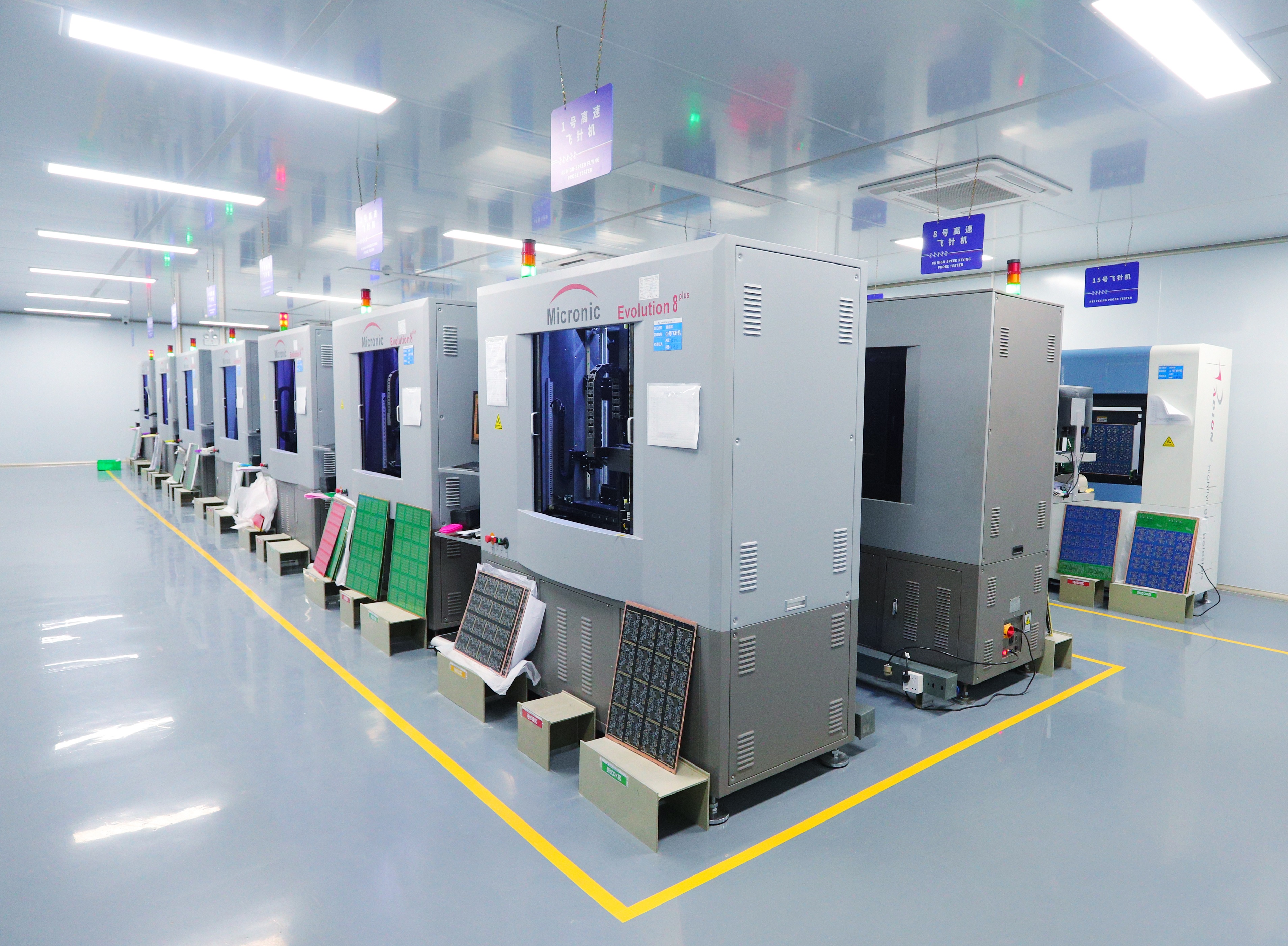
In-Circuit & Burn-In Testing
In-circuit testing checks each part and connection on the board. It uses probes to measure things like resistance and capacitance. ICT finds problems like open circuits, shorts, or wrong parts. This test gives a clear pass or fail, so boards are checked before leaving the factory.
Burn-in testing pushes boards very hard. It runs them at high heat and voltage for many hours. This finds weak parts that might break soon. Burn-in testing is important for things like planes and medical tools.
Burn-in testing copies tough conditions to find hidden problems.
It finds things like cold solder joints, bad connectors, and parts that break early.
Burn-in gives important data, like how many parts fail and how long boards last.
These tests help stop problems in the field and make sure boards last a long time.
Using AOI, ICT, and burn-in testing helps customers trust the boards. Professional PCB makers use these tests to meet rules and give boards that work well in hard places.
Plating & Finishes
Edge Plating
Edge plating is also called castellation. It covers the sides of a PCB with metal. This makes the board stronger and gives new ways to connect. Engineers use edge plating to make paths for electricity across layers. This keeps signals strong in high-frequency and RF devices. Edge plating also acts like a shield. It blocks bad electromagnetic and radio-frequency signals. This helps the board work better in noisy places.
Functional Benefit | Explanation | Importance for High-Performance PCBs |
|---|---|---|
Shorter signal paths, better signal quality | Needed for RF, telecom, and microwave applications | |
EMI/RFI Shielding | Protects circuits from outside interference | Supports EMC compliance in sensitive environments |
Thermal Management | Extra paths for heat to escape | Helps in high-power and rugged applications |
Mechanical Strength | Resists wear and edge damage | Vital for automotive and industrial electronics |
Space Efficiency | Uses board edges for connections | Frees up space for more components |
Edge plating also keeps out water and chemicals. This makes it good for tough or outdoor places. Designers can use edge plating for special board shapes or to add parts on the edge.
Vias-in-Pad & Cavities
Vias-in-pad and cavity structures help fit more parts on a PCB. They put vias right under the pads of parts. This saves space and helps with fine-pitch BGAs. It lets more parts fit and uses the board area better.
Vias-in-pad helps heat move away from hot parts.
Filled and capped vias make a flat spot for tiny chips.
Shorter signal paths help stop bad electrical effects.
Cavities let parts sit lower, so the board is thinner and cools better.
Engineers fill vias with copper or epoxy to move heat and make the board stronger. These features help PCBs work well in fast, powerful, and small designs.
Quick-Turn & Scalability
Fast Prototyping
Professional PCB manufacturers help engineers get working boards fast. Making a prototype usually takes 5-7 days. Quick-turn services can make boards in just 1-2 days, but they cost more. For example, a medical device company got boards in 2 days. This helped them find and fix problems before making many boards.
Production Stage | Typical Lead Time |
|---|---|
1-3 days (sometimes 24 hours) | |
Small Series Production | About 1 week |
Fast prototyping helps turn ideas into real products quickly. Teams can test and improve designs in short steps. This lowers risks and stops expensive mistakes. Real boards help everyone talk and share ideas better. With quick prototyping, companies get feedback early and make smarter choices.
Tip: Quick-turn prototyping helps teams work faster and stay ahead in busy fields like IoT, cars, and medical devices.
High-Volume Production
When making lots of boards, makers must keep quality high. They use careful checks like looking at boards, AOI, X-ray, and electrical tests. These steps catch problems early and make sure boards meet rules like ISO 9001 and IPC-A-600.
Quality inspectors check every step.
Special tools like 3D AOI and AI find tiny problems.
Regular checks and training keep work up to date.
Big orders also use real-time systems for quick fixes. These controls help make strong PCBs fast, which is needed for industries that want both speed and accuracy.
Why Professional PCB Manufacturers Matter
Certifications & Compliance
Professional PCB Manufacturers are very important for big projects. They follow tough rules and have special certificates for quality and safety. These certificates show that every board is safe and works well for things like planes, hospitals, and cars.
Certification / Standard | Description | Importance for High-Reliability Markets |
|---|---|---|
Highest reliability for rigid PCBs, tight tolerances, strict testing | Essential for aerospace, military, and medical devices | |
Quality management for medical devices, traceability, defect control | Mandatory for medical PCBs, ensures regulatory compliance | |
Safety and reliability testing, covers electrical and environmental factors | Validates safety for automotive, aerospace, and medical industries | |
Design, assembly, and repair process standards | Supports consistent quality and reliability |
Professional PCB Manufacturers also work with groups like UL to check for safety. They test boards for electricity, strength, and the environment. Their certificates help people trust that each board will work safely in hard places.
Experience with Complex Designs
Professional PCB Manufacturers know how to make hard PCB designs. Their engineers know how to handle tough problems. They use smart computer tools to see how boards will act under stress. This skill helps stop big mistakes and saves time.
Good technical help makes designs easier to build.
Testing in the factory finds problems early and lowers risk.
Good supply chains stop part shortages and slowdowns.
Clear paperwork and tracking help keep quality high.
Professional PCB Manufacturers use their skills to keep signals strong and power steady. They know how to fit lots of parts in small spaces. Their knowledge helps every project meet tough goals. Customers get boards they can trust, with fewer problems and faster delivery.
High-performance uses need special skills and strong trust. Professional PCB Manufacturers make sure boards are always good by following strict rules. They use advanced tests and strong steps to check quality.
Evaluation Aspect | Key Considerations |
|---|---|
ISO 9001, IPC, UL | |
Testing | AOI, ICT, Burn-In |
Service | Fast response, DFM reviews |
Tip: Check for certifications, testing, and good communication before picking a partner.
FAQ
What industries benefit most from advanced PCB manufacturing?
Industry | Application Examples |
|---|---|
Aerospace | Avionics, satellites |
Automotive | ADAS, EV power systems |
Medical Devices | Imaging, monitoring systems |
Telecom | 5G, RF modules |
How do professional PCB manufacturers ensure product reliability?
They use strong tests like AOI, ICT, and burn-in. These tests find problems early. This helps make sure boards work well in hard places.
Can manufacturers handle both prototypes and large orders?
Yes, they make prototypes fast for quick feedback.
They can also make many boards with steady quality and good control.
See Also
Capabilities Of PCB Fabricators And LT CIRCUIT’s Complex Solutions
Creating High-Performance Printed Circuit Boards For LED Uses
Various Industry Uses For Multilayer Printed Circuit Boards
Understanding The Characteristics Of High-Speed Printed Circuit Boards