Top Strategies to Minimize Back Drilling Expenses in HDI PCB Boards
Back drilling enhances signal performance in HDI PCB boards by eliminating unnecessary copper remnants. This advanced technique, known as HDI PCB board back drill, can increase production costs. However, partnering with LT Circuit ensures innovative solutions that maintain the functionality and affordability of HDI PCB boards.
Key Takeaways
Improve your PCB design to avoid extra back drilling. Use fewer blind and buried vias to make the layout simpler and signals clearer.
Use better drilling tools like laser drills. These tools are more accurate and work faster, saving money over time even if they cost more at first.
Work with experienced manufacturers like LT Circuit. Their skill in precise drilling gives good results and keeps costs low.
Understanding HDI PCB Board Back Drill
What is Back Drilling in HDI PCBs
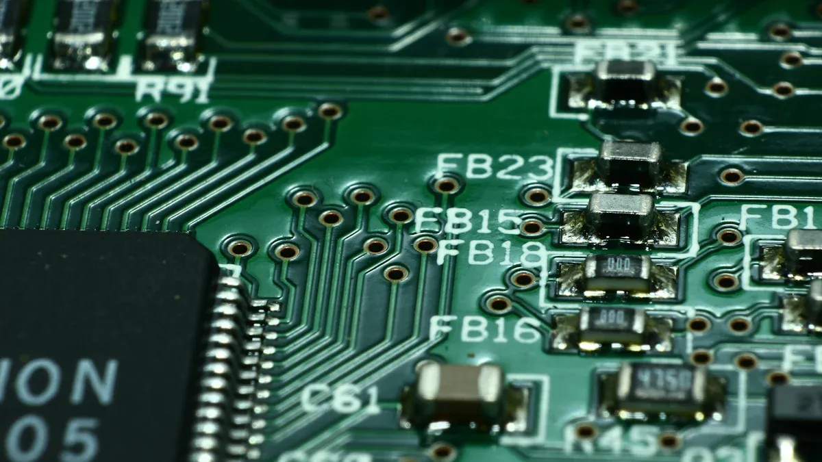
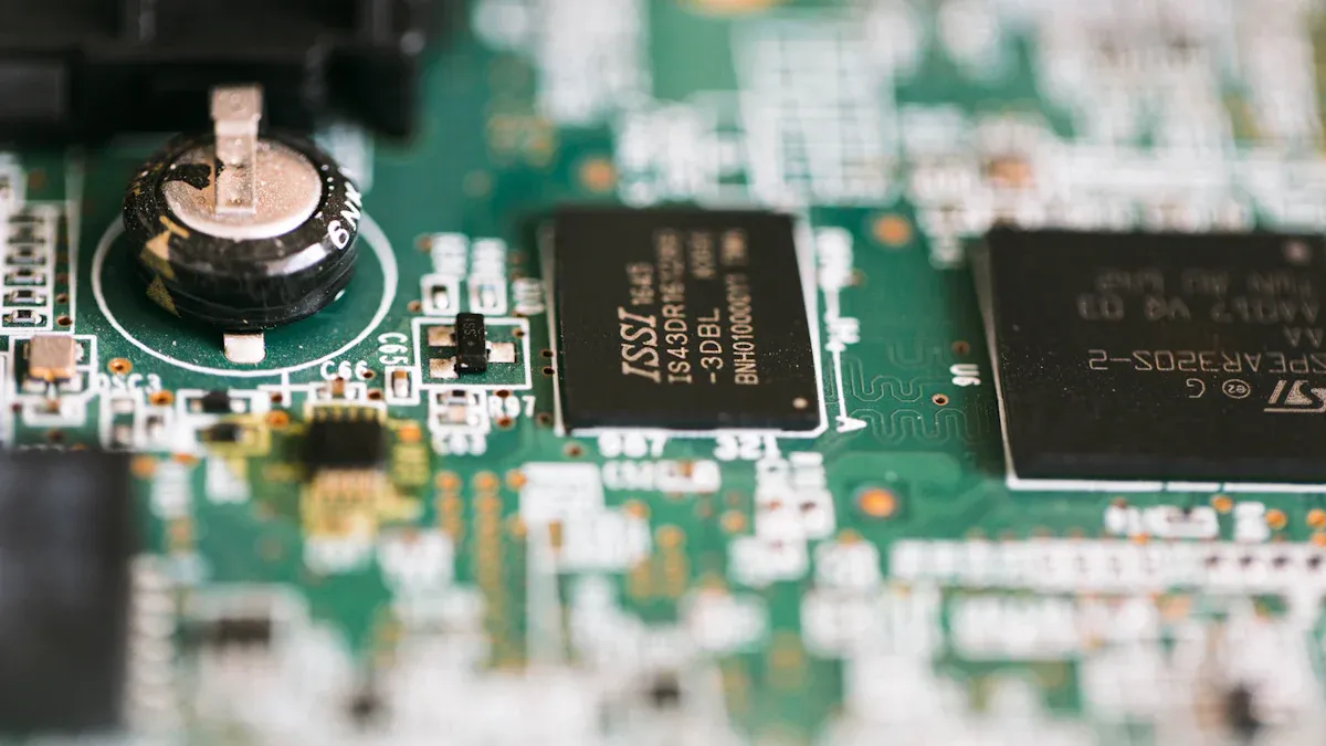
Back drilling removes extra copper from holes in HDI PCBs. This helps signals stay stable by cutting out unused copper, called via stubs. It’s used in multi-layer boards where signals move between layers. The process drills a hole slightly bigger than the original to remove the stub. This is called controlled depth drilling (CDD) because it needs precise depth control. For high-frequency boards, back drilling stops signal loss and boosts performance.
Importance of Back Drilling for Signal Integrity
Signal quality is very important in HDI PCBs, especially for fast designs. Back drilling reduces signal problems caused by via stubs, like noise and interference. It shortens the signal path, making signals clearer and reducing errors. This method also lowers electromagnetic interference (EMI) and stops resonance issues. It improves impedance matching, which prevents signal weakening. Boards running above 1GHz need back drilling for better performance.
Challenges Associated with Back Drilling
Back drilling can be tricky during manufacturing. Metal inside holes and board structure can block drilling. Burrs and copper wires may cause problems with accuracy. The size of the drill and hole also affects success. Adjusting drill settings and angles can fix these issues. Testing for heat stress and soldering ensures the board works well and meets standards. This keeps signals strong and production smooth.
Key Cost Factors in Back Drilling
Material Costs in HDI PCB Manufacturing
Material costs make up a big part of PCB expenses. The materials used, like special copper or laminates, affect the price. For HDI boards, the stackup design is very important. Things like layer count and via types (microvias, blind, or buried) change material needs and costs.
The table below shows how material costs are divided:
Cost Component | Percentage of Total Cost |
|---|---|
Bill of Material Cost | 61% |
Cost of PCB material and fabrication | 23% |
Cost of Component Assembly | 13% |
Tooling Costs | 3% |
Picking the right materials and stackup design can save money. This helps lower costs while keeping the board's quality high.
Equipment and Technology Investments
Back drilling needs expensive tools for production. Machines like mechanical drills cost less but are less accurate. Laser drills are more precise but cost more to use. Advanced methods like controlled depth drilling (CDD) also raise costs.
The type of vias and how they’re filled need special tools. This adds to the overall expense. Choosing the best tools for your needs can balance cost and performance.
Labor and Process Complexity
Back drilling is a detailed process needing skilled workers and tools. Steps like impedance control and Automated Optical Inspection (AOI) ensure quality but raise labor costs. These tasks often need extra training and resources, making production more expensive.
Simplifying the process and using automation can cut labor costs. Working with skilled manufacturers also reduces mistakes and boosts efficiency.
Cost-Saving Back Drilling Strategies
Improve PCB Design to Lower Back Drill Needs
Changing your PCB design can save money on back drilling. Planning the layout well reduces extra drilling and boosts efficiency. Focus on these important design points:
Design Metric | Description |
|---|---|
Makes the design simpler and avoids signal problems. | |
Keep space between backdrill holes and signal paths | Stops signal issues and keeps signals clear. |
Control how deep and precise drilling goes | Only drill where needed to avoid damaging signal paths. |
Check dielectric thickness | Stops drilling into areas that should stay untouched. |
Plan layer stack-up smartly | Helps organize the PCB to need less back drilling. |
For high-frequency boards, back drilling is key to stopping stub problems. This is especially true for signals over 3-5 GHz. Place vias carefully near important parts to avoid signal mixing and keep signals strong. Following these tips saves money and ensures good back drilling results.
Use Better Drilling Tools
Using advanced tools can make drilling more accurate and cost-effective. Controlled-depth drilling targets only the needed areas, saving materials and cutting mistakes.
Laser drilling is more exact than older mechanical drills. While it costs more upfront, it offers long-term benefits like:
Smaller designs that save space.
Long-term savings by improving system efficiency.
HDI PCBs cost more than regular boards but work better and last longer. Investing in these tools ensures good back drilling and efficient production.
Work with Skilled Manufacturers Like LT Circuit
Teaming up with skilled manufacturers helps cut back drilling costs. LT Circuit, for example, is great at making advanced PCBs and offers custom solutions. They are experts in controlled-depth drilling and design for fabrication, ensuring quality while saving money.
By working with a trusted company, you get:
Experts who know how to handle back drilling challenges.
Advanced tools and methods to simplify production.
Custom solutions that fit your needs perfectly.
Partnering with LT Circuit lowers costs and ensures your PCBs are reliable and high-performing.
Make Production Processes Simpler
Simplifying production steps can save time and money. Automating tasks and using low-cost methods improve efficiency. Ordering PCBs in bulk also reduces costs and waste.
Controlled-depth drilling helps avoid mistakes and material loss. Designing PCBs with manufacturing in mind also cuts costs by aligning the layout with production needs.
Tip: Check your production process often to find ways to improve. Small changes can lead to big savings over time.
By using these strategies, you can save money on back drilling while keeping your PCBs high-quality and functional.
Best Practices for Implementing Back Drilling
Check Your PCB Design Carefully
Reviewing your PCB design is very important for back drilling. By checking the layout early, you can spot problems and avoid costly errors. Design for Manufacturing (DFM) rules help make designs that are easy to build and work well.
When reviewing, focus on key factors that affect back drilling. The table below shows important things to check:
Parameter | Description |
|---|---|
Trace Width | Must follow size rules to avoid problems. |
Clearances | Keep enough space between parts for reliability. |
Hole Sizes | Make sure holes are the right size for drilling. |
Annular Ring Size | Should be big enough to keep connections strong. |
Follow these tips to improve your design:
Use whole numbers for all drill sizes.
Update hole names and via details in the drill chart.
Ensure pad sizes are bigger than the hole diameter.
Keep at least 6 mils of space between vias.
These steps help your design meet industry standards like IPC-A-610 and IPC-A-600. These rules ensure your PCB is reliable and high-quality.
Choose Good Materials and Tools
The materials and tools you use affect back drilling costs and quality. Strong materials like advanced copper laminates make PCBs last longer. Precise tools, like laser drills, give better results and fewer mistakes.
Good tools may cost more at first but save money later. For example, controlled-depth drills only remove what’s needed, saving material and time. Always pick quality over cheap options for the best results.
Train Your Team on Drilling Skills
Your team’s skills are key to good back drilling. Training helps workers learn how to set up tools and drill correctly. This reduces mistakes, saves time, and lowers costs.
Focus training on these areas:
Setting up and adjusting drilling tools properly.
Spotting and fixing problems during production.
Following safety rules to keep everyone safe.
Hold regular training sessions to teach new techniques. A skilled team makes better PCBs and speeds up production.
Watch and Improve Production Steps
Keep track of your production process to find problems and fix them. Use data like defect rates and production times to see what needs improvement.
Automated tools like Automated Optical Inspection (AOI) check PCBs for quality. Regular checks help you adjust to changes and keep your products reliable.
Tip: Review your production process often to find small fixes. These small changes can save a lot of money over time.
By using these best practices, you can make better PCBs, save money, and keep your production efficient.
Cutting back drilling costs in HDI PCBs improves performance and saves money. You can do this by designing smarter, using better tools, and working with experts. New ideas like mixing materials and AI design tools can save more over time.
Metric | Value |
|---|---|
Fast shipping delivery | |
Prototype making time | Within 24 hours |
Complex prototype time | Up to 3 days |
Full production time | 10 days |
Teaming up with LT Circuit gives you affordable, expert solutions you can trust.
FAQ
What is the main advantage of back drilling in HDI PCBs?
Back drilling makes signals clearer by removing extra copper. It reduces noise and interference, helping the board work better.
How can you lower back drilling costs?
Plan your PCB design carefully to avoid extra drilling. Use better tools and work with skilled companies like LT Circuit to save money.
Why pick LT Circuit for your PCB needs?
LT Circuit provides smart solutions and expert help. They make high-quality PCBs that fit your needs without costing too much.
See Also
Understanding Back Drilling Techniques in HDI PCB Production
Ten Strategies for Reducing Expenses in Custom PCB Manufacturing
Utilizing Quick Turn HDI PCBs to Lower Project Costs in 2025
Techniques for Achieving Flat Electroplating in HDI PCB Laser Drilling