Essential Tips for Reliable Power Distribution Networks in High-Speed PCB
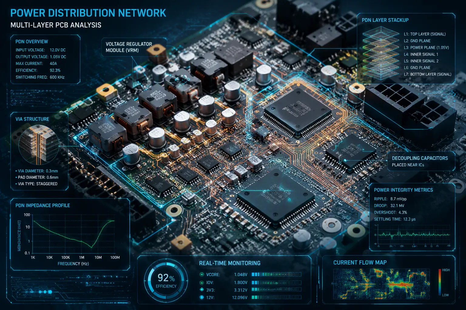
A robust power distribution network forms the backbone of every high-speed circuit board. You face a constant battle against voltage droop, noise, and signal integrity failures. Smart choices in your pcb design prevent these problems before they start. You need reliable power distribution networks to achieve stable and reliable delivery of power across every component. Clean, stable power keeps your high-speed signals intact and your system running without errors. This guide delivers practical, field-tested techniques for your pcb design workflow. You will learn how to build a power delivery system that performs under real-world conditions, not just in theory.
Key Takeaways
Calculate target impedance for each design to avoid over- or under-designing your power distribution network.
Place decoupling capacitors within 1-2 mm of IC power pins to minimize loop inductance and maximize noise filtering.
Use thin dielectric spacing between power and ground planes to increase interplane capacitance and reduce high-frequency impedance.
Route power and ground planes close together to create natural capacitance that suppresses high-frequency noise.
Use multiple vias for power and ground connections to reduce inductance and improve current flow.
Simulate your power distribution network before manufacturing to catch voltage drops and impedance peaks early.
Never split the ground plane; keep it solid to provide a low-impedance return path and reduce EMI.
Manage heat with thermal vias and wider traces to prevent resistivity increases and voltage drops.
PDN Fundamentals in High-Speed PCB
Power Integrity and Signal Integrity
Defining Power Integrity
A power distribution network in pcb design delivers stable voltage from your regulator to every IC on the board. This network includes voltage regulator modules, bulk capacitors, ceramic decoupling capacitors, power and ground planes, vias, traces, and package interconnects. Each element plays a specific role in controlling noise and meeting dynamic current demands.
Power integrity means your PDN keeps supply voltage within acceptable tolerance under all operating conditions. Voltage regulator modules typically hold output within plus or minus two to five percent. When your PDN fails to maintain this tolerance, the entire system becomes vulnerable.
PI Impact on Jitter and Errors
Poor power integrity directly degrades signal quality. PDN noise, including voltage ripple and ground bounce, modulates signal thresholds and timing. This modulation causes jitter and bit errors in your high-speed links. Ground bounce from package and via inductance shifts local ground levels and erodes timing margins.
Signal return currents flow through the PDN itself. High-frequency PDN impedance and plane splits increase loop area, crosstalk, and radiation. These effects further harm jitter and bit error rate. A low-impedance PDN with proper decoupling keeps supply noise low enough to protect both power integrity and signal integrity.
Stack-Up and Power Distribution Network
Assigning Power and Ground Planes
Strategic placement of power and ground planes across layers is critical for effective power distribution. Place power planes near high-current components such as processors or FPGAs to minimize voltage drops. In a four-layer stackup, a ground plane on Layer 2 and a power plane on Layer 3 give signal layers immediate access to a reference plane.
Power planes and ground planes are important for more than just distribution of supplying power. When defining reference planes, both with impedance controlled routing and in managing return paths, the stackup might force return currents to pass into a PCB power plane before being coupled back to a ground layer.
Always use a solid ground plane directly below controlled-impedance traces. Avoid splits and gaps that disrupt return paths and create noise.
Thin Dielectrics for Decoupling
Position power and ground planes close together on thin dielectric layers. This tight spacing increases natural interplane capacitance and reduces PDN impedance at high frequencies. The plane pair acts as a distributed capacitor that handles noise above the range where discrete capacitors become ineffective.
Target Impedance Basics
The Golden Rule of PDN Design
Target impedance is the maximum impedance allowed between the IC die and its power rail. If your PDN stays below this value, worst-case transient current produces only acceptable supply-voltage noise. Calculate it as Z_target = V_dd × ripple_tolerance / I_max_transient. For an FPGA with V_dd = 0.9 V, 3% ripple (27 mV), and 2 A transient current, Z_target = 13.5 mΩ. There is no single universal target impedance value; calculate it for each design to avoid over-designing or under-designing the PDN.
Impedance vs. Frequency
Your PDN must meet target impedance from DC up to the highest transient frequency. The VRM controls DC to 1 MHz. Bulk and ceramic capacitors control 1 to 100 MHz. The PCB power and ground plane pair controls 100 MHz to 1 GHz. IC on-die capacitance controls above 1 GHz. Impedance peaks from resonances and anti-resonances should be avoided in that band.
Core Strategies for Reliable Power Distribution Networks
Decoupling Strategy
Choosing Capacitor Values
You must select capacitor values based on the frequency range each capacitor addresses. Mix values such as 0.1 µF, 1 µF, and 10 µF to handle both high-frequency and low-frequency noise. Do not blindly place 0.1 µF everywhere. A well-sized bulk capacitor provides energy storage for low-frequency demands. A single properly selected decoupling capacitor handles the relevant high-frequency range near the power pin. Avoid copying many different values in parallel. Parasitic inductance and LC resonances can create impedance peaks rather than flattening PDN impedance.
Frequency range | Selection guidance |
|---|---|
Low-frequency / bulk energy storage | Use a well-sized bulk capacitor for energy storage instead of replicating many low-value capacitors. |
High-frequency / IC switching | Use a single properly selected decoupling capacitor for the relevant high-frequency range, placed close to the power pin. |
Multiple frequency ranges in parallel | Avoid copying many different values in parallel because parasitic inductance and LC resonances can create impedance peaks rather than flattening PDN impedance. |
Placement and Mounting
Place decoupling capacitors as close as possible to IC power pins. This placement minimizes loop inductance and maximizes noise filtering. Optimize the current path rather than only minimizing distance. Connect the component pin to the capacitor first and then to the via. This sequence ensures a short current path for noise filtering and low impedance. Use multiple vias to connect decoupling capacitors to power and ground planes. Multiple vias minimize loop area and via inductance. Place capacitors directly on the power plane through short vias to avoid trace stubs. For BGAs, place decoupling capacitors under the BGA or on the opposite side across the BGA periphery. Use via-in-pad technology to connect capacitors directly to BGA power pins. Share vias between adjacent power or ground balls only when acceptable. Avoid more than two balls per via to maintain low impedance.
Bulk, Bypass, and High-Frequency Caps
Give each power supply rail its own set of decoupling capacitors. Different rails have different current demands and impedance requirements. Prioritize low-value capacitors near power pins. Use bulk capacitors nearby for transient current demand. Add a bulk capacitor of 10 µF or higher near the power entry for sudden current demands. Use short, wide traces or direct vias to the ground plane. Long traces add inductance and hurt high-frequency decoupling. At high frequencies, capacitance value matters less than inductance.
Shared vias add shared inductance directly into the high-di/dt current path, raising PDN impedance at the frequencies that matter. Independent vias allow solid power/ground planes to form the lowest-inductance connection between the IC and its decoupling capacitor.
Optimizing Power and Ground Planes
Low-Inductance Plane Pairs
Adjacent power and ground planes create inherent interplane capacitance and very low parasitic inductance. This low capacitance supports very high-speed switching events and helps maintain low PDN impedance. This approach is a better high-frequency solution than discrete capacitors. Place power and ground planes close together on thin dielectric layers. Tighter plane spacing increases interplane capacitance and reduces high-frequency impedance. A 4 mil spacing versus 8 mil prepreg between power and ground significantly increases this built-in capacitance. This directly improves reliable power distribution networks by ensuring low-impedance power delivery at high frequencies where decoupling capacitors become less effective.
Interplane Capacitance Benefits
Interplane capacitance between power and ground planes behaves as many distributed infinitesimal capacitors. It is the only practical decoupling approach above 500 MHz and also remains effective down to about 50 MHz. Above 50 MHz, about 1000 pF per square inch is needed. Ordinary 5-10 mil plane spacing provides only 1/5 to 1/10 of that amount. A 2-mil ZBC-2000 laminate gives 500 pF per square inch. Two power/ground plane pairs can provide the required 1000 pF per square inch. Placing power and ground planes adjacent creates a natural capacitance of approximately 1 nF per square inch. This natural capacitance aids in high-frequency noise suppression. Because the planes act as distributed capacitance, the exact placement of discrete decoupling capacitors is less critical. Capacitors should still be spread evenly across the board to support transient current demands.
Trace and Via Optimization
Wide Traces and Multiple Vias
Use multiple power and ground vias to create parallel current paths and reduce inductance. Via stitching improves power distribution between layers. Long via structures or too few vias increase inductance and restrict current flow. Keep power paths short and direct through strategic component placement and optimized routing. Long power routes increase resistance and inductance, reducing power delivery efficiency. Use solid power and ground planes with adequate copper area. Narrow power paths, fragmented planes, and inadequate copper areas increase resistance and cause voltage drops. Closely coupled power and ground layers lower impedance.
Back-Drilling Via Stubs
Back-drilling removes unused via stubs from high-speed signal vias. These stubs act as unterminated transmission line segments. They cause reflections and degrade signal integrity at high frequencies. Back-drilling eliminates this stub effect and improves signal quality. This process supports the low-inductance return path your high-speed signals require. A clean via structure also reduces crosstalk and electromagnetic radiation. Apply back-drilling to critical high-speed nets where stub length becomes a significant fraction of the signal wavelength.
Practical PDN Design Tips
Component Placement and Routing
Capacitors Near IC Pins
Place decoupling capacitors as close as possible to IC power pins. This single practice minimizes the high-frequency current loop and loop inductance. A capacitor beside the IC power pin acts as a local energy reservoir. It supplies charge quickly during sudden switching-current bursts. If the capacitor sits farther away, PCB trace inductance and resistance delay current delivery. Even a few millimeters of extra trace can reduce effectiveness and cause brief voltage drops or logic errors. Connect capacitors directly to power and ground planes and avoid long routing. Short, wide connections reduce loop area and parasitic inductance. On four-layer boards, keep capacitors on the same side as the IC and pair power and ground vias tightly. For BGA, FPGA, and CPU packages, minimize distance from power pins and use via-in-pad or backside decoupling where suitable. Low-ESL ceramic capacitors, such as X7R or X5R, respond quickly and suit this local decoupling role. These decoupling capacitor best practices protect your power distribution network in pcb performance across the full frequency range.
Routing Power Before Signals
Route the most critical signals first, then route power wires and planes. Group similar signals and those originating or terminating in the same subcircuit. Avoid running traces underneath sensitive components such as oscillators and RF modules. Always route signal-carrying traces over a suitable reference plane. Keep trace lengths short in the power distribution network to reduce parasitic inductance and resistance. A solid ground plane provides a low-impedance return path and stabilizes impedance. Never route over plane splits. Keep reference planes solid under high-speed traces. These return paths must stay continuous to prevent noise and radiation.
Impedance Control and Voltage Drop
Managing DC IR Drop
Dedicate inner layers to solid power and ground planes. Avoid splits except where isolation is essential. Perform voltage drop calculation by summing series resistances along current paths. Incorporate temperature coefficients because resistivity rises with heat. Place high-current components closer to the power source to minimize loop length. Ensure the total current drawn by various circuit blocks does not surpass the rated output capacity of the power regulator. Use remote sensing with additional leads to sense voltage at the load and dynamically adjust output. Opt for 2-3 oz copper cladding for high-current circuits to reduce resistance. Employ a stand-up bus bar to route power lines and provide a low-resistance DC path. Widen power traces proportionally to current, using IPC-2152B charts for cross-section adequacy under temperature rise limits. IPC-2221 provides power distribution, plane usage, stackup, and grounding guidance that supports stable power delivery.
Low-Impedance Paths
Use adjacent power-ground plane pairs to maximize capacitance while minimizing loop inductance. Include stitching vias every few millimeters along plane cuts for routing to maintain low impedance. Use poured copper fills on signal layers to extend effective plane area. Maintain at least 20% clearance around cutouts to preserve current flow uniformity. Select decoupling capacitors to cover the frequency spectrum: bulk caps for low frequencies, ceramic 0.1 μF types for mid-range, and smaller high-frequency caps for GHz noise. Prioritize low equivalent series inductance and match self-resonance frequency to switching harmonics. Use arrays of varied capacitor values in parallel to broaden frequency coverage. A low-impedance power distribution network keeps supply noise low enough to protect both power integrity and signal integrity. This impedance control approach directly supports a reliable pdn.
Via Placement and Stitching
Vias Near Capacitors and ICs
Arrange vias in a uniform grid pattern to prevent plane voids and hot spots. Maintain at least 15 mil spacing between vias. Place dedicated ground vias near signal vias. Position ground vias immediately adjacent to signal vias at both source and sink to provide a direct, low-inductance return path. Use multiple vias (2-4 per connection, paralleled) to cut inductance by approximately 50%. Keep capacitors within 1-2 mm of the IC pin when possible. A well-placed via can be more critical than simply placing the capacitor physically close to the IC. Use thermal via arrays under thermal pads for heat dissipation. For compact boards, use microvias or blind vias to connect planes without consuming surface area. IPC-2226 gives HDI design guidance, including microvia and lamination considerations.
Ground Plane Stitching
Never split the ground plane. Splitting forces high-frequency return currents to take long, unpredictable paths, increasing noise and EMI. Use via stitching along plane edges with pitch between λ/20 and λ/10. Place stitching capacitors of 10 nF to 100 nF at signal transition points when routing across split planes or between ground and power reference planes. This provides continuous return paths. Use stitching vias every lambda/20 along plane cuts. Avoid splits longer than a wavelength at operating frequencies. A solid ground plane and tightly coupled power and ground planes form the foundation of your decoupling strategies. These practices ensure your pdn meets target impedance across all relevant frequencies.
Advanced PDN Verification and Considerations
Simulating the Power Distribution Network
DC and AC Analysis Tools
You should validate your design with simulation before manufacturing. DC drop analysis checks voltage drops across the PDN and finds power bottlenecks. AC analysis evaluates the power plane's ability to supply stable power at high frequencies. You can estimate these quantities in schematics using SPICE or IBIS models. In the PCB layout, an electromagnetic field solver calculates them. Compare your results with target values to confirm compliance.
Several tools support this work. Siemens HyperLynx handles signal and power integrity analysis. Altium PDN Analyzer optimizes power delivery efficiency. Siemens Simcenter FloTherm provides thermal simulation. Cadence circuit simulation tools verify overall functionality. For advanced signal integrity, use SPICE and IBIS-AMI for pre-layout and post-layout analysis. Hardware tools like oscilloscopes and VNAs validate real-world performance.
Reading Impedance Curves
Your impedance curve shows whether the PDN meets target impedance across frequency. Peaks from resonances and anti-resonances reveal power integrity issues. You must flatten these peaks with proper decoupling. This pdn modeling step confirms your design works before you commit to fabrication.
EMI/EMC Mitigation
PDN Role in Reducing Radiation
A well-designed PDN reduces electromagnetic radiation and supports EMI/EMC compliance. Large signal or power loops strengthen magnetic fields and raise emissions. Split planes and long return-current detours increase loop area. Missing or poorly placed decoupling capacitors let high-frequency noise appear on power rails.
Practice | EMI/EMC benefit |
|---|---|
Do not split reference planes under transmission lines | Avoids unintentional antennas that radiate noise |
Move transmission lines closer to a suitable reference | Reduces inductance and mitigates EMI |
Split power planes, not ground planes | Yields more favorable EMI outcomes |
Place decoupling capacitors close to IC pins | A tight loop suppresses noise at the source |
Grounding and Shielding
Ground stitching around board edges creates a Faraday-cage-like containment. This technique can cut radiated emissions by up to 20 dB above 100 MHz. Edge stitching alone can add up to 10 dB reduction. Shielding cans grounded at multiple points can lower emissions by up to 30 dB below 1 GHz. Guard rings around sensitive traces reduce noise pickup by 10 to 15 dB. Space ground vias less than 1/20th of the signal wavelength, such as under 7.5 mm at 1 GHz.
Thermal Management
Heat from High-Current Traces
High-current traces generate heat that degrades your PDN. Resistivity rises with temperature, which increases voltage drop. Use wider traces and thicker copper to spread current and lower resistance. Keep high-current components near the power source to shorten loop length.
Thermal Vias and High-Conductivity Materials
Thermal via arrays under thermal pads move heat away from hot spots. Use high thermal conductivity materials to improve heat dissipation. These steps protect your pdn validation results and keep the board within safe operating limits.
Common PDN Design Mistakes
Decoupling Errors
Wrong Capacitor Values
A 10 µF capacitor handles slow voltage dips but becomes useless above a few MHz. A 0.01 µF capacitor kills high-frequency spikes but will not help at startup. Any capacitor acts like an inductor above its self-resonant frequency.
A Y5V dielectric loses capacitance with temperature shifts and DC bias. Choose X7R or X5R ceramics. Match each capacitor's self-resonant frequency to the switching harmonics you need to suppress.
Poor Capacitor Placement
Distance defeats good capacitor values. A 0.1 µF capacitor placed 2 mm from the VDD pin works well. The same capacitor placed 2 cm away might as well not be there.
Long traces from the capacitor to the IC pin add inductance. Shared vias create noisy return paths. One capacitor shared across many ICs cannot serve independent transients. Connect decoupling capacitors directly to the power and ground planes.
Plane and Stack-Up Mistakes
Split Ground Planes
A split ground plane forces return current around the gap. The detour enlarges the loop, adds inductance, and radiates EMI. Crosstalk can rise 30 percent at 1 GHz versus a continuous plane.
Keep splits minimal. Connect ground sections at a single point when needed. Use stitching vias across unavoidable gaps.
Poor Stack-Up Choices
Layer order shapes PDN impedance in pcb design. Put a solid ground plane directly below components. A power shape there leaves outer traces without a continuous reference. Every signal layer needs an adjacent ground plane.
Separating power from ground removes the plane pair capacitance. Place power next to ground on a thin dielectric, about 3 to 5 mils apart, to form that planar capacitor.
Skipping Simulation
Relying on Guesswork
Copying a previous design or a datasheet example is risky. Those designs worked under their conditions, not yours. Start with pre-layout simulation to explore the correct design space. Vendor tools like LTspice help, but you must model PCB electromagnetic parasitics and decoupling capacitors too.
Waiting until measurement to debug is expensive. Pre-layout analysis costs hours, not weeks. It reveals problems before layout locks them in.
No Pre-Fab Validation
Run power integrity simulation after board layout. It reveals anomalous impedance spikes. This adds about half a day, far less than respinning the PCB.
Real failures prove the cost. A data acquisition board delivered more than 10 dB less dynamic range than its datasheet. A motor driver board triggered undervoltage protection because a long power trace created a 0.3 V dip at startup.
Inadequate power integrity analysis can reduce device performance and reliability. Uneven power distribution and increased noise can cause system disruptions and potentially damage components. Addressing power integrity issues early helps improve PCB performance and longevity.
A reliable power distribution network is a foundational requirement in high-speed PCB design, not an afterthought. You must treat target impedance, strategic decoupling, solid stack-up, via optimization, and simulation validation as core workflow steps. Place decoupling capacitors close to IC power pins to suppress switching noise. Use solid power and ground planes for low-impedance delivery. Minimize current loop paths to cut inductance and EMI. Run SPICE simulation before fabrication to catch voltage drops and instability early. These habits build reliable power distribution networks that protect signal integrity. A well-designed PDN directly drives your product's success in the market.
FAQ
How do you calculate target impedance for a power distribution network?
Use the formula Z_target = V_dd × ripple_tolerance / I_max_transient. For an FPGA with 0.9 V supply, 3% ripple, and 2 A transient current, target impedance equals 13.5 mΩ. Calculate this value for each design. No universal target impedance exists.
How close should decoupling capacitors sit to IC power pins?
Place capacitors within 1-2 mm of the IC pin when possible. A capacitor placed 2 mm away works well. The same capacitor at 2 cm provides almost no benefit. Short connections minimize loop inductance and maximize noise filtering.
Why does thin dielectric spacing between power and ground planes matter?
Tight plane spacing increases interplane capacitance and reduces high-frequency impedance. A 4 mil spacing versus 8 mil prepreg significantly boosts this built-in capacitance. This approach handles noise above the range where discrete capacitors become ineffective.
What problem does back-drilling solve in high-speed vias?
Back-drilling removes unused via stubs that act as unterminated transmission line segments. These stubs cause reflections and degrade signal integrity at high frequencies. Apply back-drilling to critical high-speed nets where stub length becomes a significant fraction of signal wavelength.
When should you run PDN simulation during the design process?
Start with pre-layout simulation to explore the correct design space. Run power integrity simulation after board layout to reveal anomalous impedance spikes. This adds about half a day, far less than respinning the PCB. Pre-layout analysis costs hours, not weeks.
Why should you never split the ground plane?
Splitting forces high-frequency return currents to take long, unpredictable paths. This increases noise and EMI. Crosstalk can rise 30 percent at 1 GHz versus a continuous plane. Keep splits minimal and use stitching vias across unavoidable gaps.
How do thermal vias protect your PDN performance?
Thermal via arrays under thermal pads move heat away from hot spots. High-current traces generate heat that degrades your PDN because resistivity rises with temperature. Use high thermal conductivity materials to improve heat dissipation and keep the board within safe operating limits.
