Reliable Signal Integrity and EMI Control in High-Speed PCB

A failed EMC certification can stall your product launch, force board respins, and pile on extra testing costs. These failures rank among the most costly issues in hardware development.
EMC failures found during compliance testing frequently necessitate board respins and cause schedule slippage.
So how do you manage reliable signal integrity while controlling electromagnetic interference? The answer lies in disciplined pcb design. You must control impedance, route return paths, and decouple power. Every choice affects signal integrity. Engineering evaluations before regulatory testing increase confidence in production readiness. Embedding compliance throughout development lowers redesign cycles. Your pcb layout, grounding, and shielding determine first-pass certification success.
Key Takeaways
Start with a solid layer stackup and component placement to lock in signal integrity and EMI performance.
Keep return paths continuous to avoid signal integrity problems and reduce electromagnetic radiation.
Route controlled impedance traces with uniform width and spacing to prevent reflections and crosstalk.
Place decoupling capacitors close to power pins to reduce noise and stabilize power delivery.
Use via stitching and ground planes to minimize loop area and suppress emissions.
Apply shielding and filtering techniques to contain EMI after layout and grounding.
Simulate signal integrity and EMI before layout, then verify with measurements after prototyping.
Learn from real-world cases: fix stackup, routing, and grounding issues to pass compliance and improve performance.
Layout and Stackup in High-Speed PCB Design
Your stackup and placement decisions lock in most signal integrity and EMI outcomes before you route a single trace. Get these fundamentals right, and the rest of your high-speed pcb design becomes far more forgiving.
Layer Stackup Selection
Signal, Ground, and Power Layers
Determine your layer count from routing density and the number of unique voltage domains. Assign outermost layers as signal layers when possible, or reserve them for components and low-speed signals while dedicating inner layers to high-speed routing between planes. Place solid, unbroken ground planes on layers immediately adjacent to critical signal layers. Locate power planes adjacent to ground planes so the pair forms a low-inductance capacitor for high-frequency decoupling. Consider routing direction on adjacent layers — orthogonal routing between layers separated by a plane reduces broadside crosstalk. These practices reduce the need for extensive post-layout simulation and help your board meet performance targets on the first fabrication iteration.
Controlled Impedance and Dielectrics
Select trace widths and dielectric thicknesses to achieve target impedances, typically 50 Ω single-ended or 100 Ω differential, while maintaining symmetry in the build-up to control warpage. Thicker copper lowers characteristic impedance, so you must compensate by widening traces or increasing dielectric thickness while modeling copper roughness and etch factor in a field solver. Use finished copper thickness, not nominal foil weight, in impedance calculations because outer-layer plating adds 20–30µm. Ignoring this yields consistently low impedance at fab.
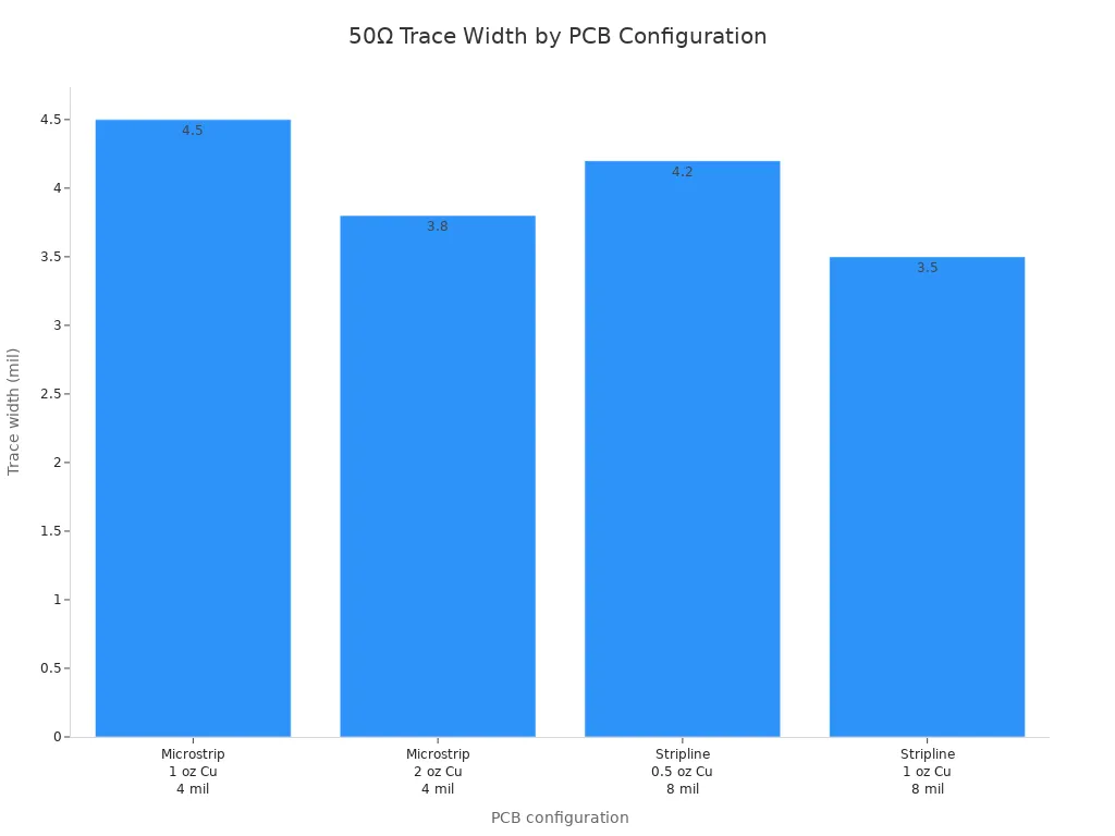
Keep signal layers at 0.5oz; heavy 2oz copper on signal layers forces wider traces and wastes routing density. When mixing copper weights, specify high-flow prepreg or add copper-balancing patterns because standard prepreg cannot fill step changes uniformly. Test coupons in the panel should verify the modeled impedance after fabrication.
Component Placement
Separating High-Speed, Analog, and Power
Follow schematic signal paths when creating the floorplan. Place sensitive analog components in the analog section and noisy digital components in the digital section to avoid shared return paths. Route digital vias only within the digital zone, away from analog circuit areas. Place a row of ground vias along the analog/digital boundary to create a physical barrier that blocks EMI from crossing between sections. Keep vias at least 0.5 mm away from high-speed digital components to stop them from acting as antennas. Isolate power modules from the rest of the circuit while keeping them close to the components they power.
Clock and Connector Positioning
Treat sampling clock generation circuitry as an analog section with proper grounding and decoupling. Isolate it from noisy digital circuits. Route clock traces away from noisy components and use differential clock signals. Place connectors along the board edge and keep supporting components like decoupling capacitors and crystals as close as possible to the mixed-signal devices. Keep power traces short, direct, and wide to reduce inductance.
Reference Plane Integrity
Avoiding Plane Splits
A continuous copper plane provides the lowest-impedance return path at high frequencies. Return current tends to flow directly beneath the signal trace to minimize loop area. Any gap, slot, or split in the plane forces the return current to detour, increasing inductance and creating potential antennas for EMI. When a signal trace crosses a split, the return current cannot flow directly beneath the trace and must detour around the discontinuity. This detour increases the current loop area, which raises inductance and makes the loop a more efficient radiator. Disrupted return paths can worsen ground bounce and crosstalk when return currents share inductive paths or couple with adjacent signals. Provide a return current bridge across any required split using stitching capacitors, a narrow copper connection, or route the signal over a different continuous reference plane. For layer transitions, place stitching vias between reference planes near the signal via to provide a low-inductance return path.
The 20H Rule for Edges
Offset power planes from board edges to reduce edge radiation. The 20H rule recommends setting back the power plane from the board edge by twenty times the dielectric thickness between the power and ground planes. This setback reduces fringing fields that escape from the board edge and radiate. Apply this rule consistently across all power planes in your layer stack-up.
Routing for Signal Integrity in PCB Design
After stackup and placement, trace routing becomes your main control over signal integrity in pcb design. Controlled impedance traces prevent reflections. Poor routing creates impedance mismatches and large return loops. Large loops amplify electromagnetic coupling and crosstalk. Routing choices for high-speed pcb design must therefore manage signal integrity and crosstalk and emi together.
Controlled Impedance Routing
Trace Width, Spacing, and Dielectrics
A transmission line must present constant impedance along every millimeter. Keep a solid reference plane adjacent to every signal layer. Plane splits create local impedance discontinuities. Keep trace width uniform; if necking down is unavoidable, minimize its length. Sudden width changes produce impedance mismatches. Use 45-degree or arc bends instead of 90-degree corners. Maintain enough spacing from neighboring traces and copper pours. Parasitic capacitance from close neighbors changes effective impedance. For differential pairs, route both legs with uniform spacing. Do not place components or vias between the pair. Place AC-coupling capacitors symmetrically. Use a laminate with stable Dk and a symmetrical stackup. These steps keep controlled impedance closer to target. Verify manufactured impedance with TDR coupons.
Length Matching and Skew Budgets
Parallel buses require all bits to arrive within one bit interval. Skew destroys timing margin. Match each trace group to the same physical length, not just the same delay specification, because signal velocity depends on dielectric constant. Match both legs in differential pairs. Place serpentine compensation near the source of mismatch. Route high-speed traces over a continuous reference plane and away from pcb edges. Edge proximity changes impedance. Length matching delivers high-speed signal integrity.
Crosstalk and Coupling Control
The 3H Rule for Spacing
Crosstalk appears when fields from one trace couple into another. Coupling strength drops as separation grows. The 3H rule recommends spacing traces at least three times the dielectric height above the nearest plane. This limits near-end and far-end crosstalk. Doubling spacing halves near-end crosstalk. Trace width no longer matters after traces exceed critical length; only edge-to-edge separation and height matter. Keep inter-pair separation at least five times the intra-pair gap. On adjacent layers, route traces orthogonally, X on one layer and Y on the other. Guard traces can shield critical clocks; connect them to ground or a reference voltage. Simulation can quantify this relationship for your specific stackup.
Via Stub and Layer Transition Control
Every via adds a capacitive discontinuity. A via stub can act as a resonant antenna. Back-drill long stubs or reduce layer changes. When transitioning, place a ground via near the signal via. Unequal spacing between ground and signal vias causes mode conversion. That mode conversion increases common-mode noise and EMI. Keep transitions symmetrical. Limit layer changes; each adds an impedance mismatch. For differential pairs, transition both lines together. Stub length above the receiving pin matters as much as the stub below it.
A high-speed signal crossing a split plane, void, or reference transition without a nearby return via can create radiation, crosstalk, mode conversion, and ringing.
Termination for Signal Integrity in PCB Design
Series, Parallel, and Differential Termination
Impedance mismatches produce reflections at driver and receiver. Termination absorbs excess energy. Series termination places a resistor near the driver. Choose its value so resistor plus driver output impedance equals trace impedance: Zst = Zo - Zout. Parallel termination places a resistor near the receiver, with value matching line impedance. Thevenin termination uses two resistors whose equivalent matches trace impedance. AC termination adds a capacitor; it works over a wide frequency range. Bidirectional termination places resistors at both ends for multipoint buses. Each scheme has trade-offs between power, cost, and board space. Differential lines need a resistor equal to differential impedance across the pair. A 124-ohm differential cable requires a 124-ohm resistor; single-ended use needs half that value. Good termination assumes controlled impedance along the trace.
Return Path Continuity
Return path continuity decides signal integrity in pcb. Termination cannot fix a broken return path. Cutouts, slots, or clearance holes interrupt the return path. The loop area expands. Larger loop area increases inductance. Return current spreads toward board edges and radiates. This links poor routing to both signal integrity in pcb and EMI. Keep a continuous ground plane under every high-speed signal. Provide return vias near signal vias at transitions. If a split is unavoidable, bridge it with a stitching capacitor. Stitching vias along a split boundary also suppress edge radiation. Run signal integrity analysis during pcb layout. Pre-layout signal integrity analysis shows where return current will detour. Post-layout checks confirm stitching and via placement. Together, these steps protect signal integrity in pcb design and prevent compliance failures. High-speed pcbs demand this discipline. For signal integrity in pcb, the return path is the foundation. Return path continuity is a core principle of signal integrity in pcb design.
Grounding and Decoupling for Reliable Signal Integrity
A solid and continuous ground plane is the foundation of reliable signal integrity and EMI control. It creates a low-impedance return path directly beneath every signal trace. Place signal layers next to reference planes, and return currents follow the path of least impedance. This arrangement shrinks loop area, reduces voltage fluctuation, and suppresses radiation and switching noise. Solid power and ground planes also lower impedance in the power distribution network. Proper via and plane placement improves current return efficiency and power stability. Filtering near noise sources complements decoupling, but grounding comes first.
Grounding Schemes
Single-Point Versus Multi-Point
Single-point grounding uses long traces, so its impedance climbs at high frequencies and those traces act as antennas. Multi-point grounding ties circuits to a plane and delivers very low impedance, excellent EMI performance, and simple implementation. Choose single-point grounding only for very simple, low-frequency circuits where a plane is not feasible. Choose multi-point grounding for most analog and mixed-signal applications, especially high-frequency or complex designs.
Analog and Digital Return Partitioning
Mixed-signal boards need deliberate ground plane strategies. Designate separate analog and digital areas, then connect them at one point near the ADC, DAC, or power supply. This avoids ground loops while keeping a common reference. Keep analog and digital signals on separate layers or regions. Never run digital traces over the analog ground plane, because capacitive coupling injects noise. Place decoupling capacitors such as 0.1 μF ceramic parts close to digital power pins to shunt high-frequency noise to ground. Think in current loops, not plane areas. Keep digital loops short and away from sensitive analog return paths, and cluster analog blocks near their converter inputs to limit shared return impedance.
Power Delivery Network
Target Impedance and Capacitor Selection
At DC, a power path shows low impedance dominated by resistance. As frequency rises, inductance dominates and path impedance climbs. A high-impedance path droops when a device demands current suddenly, and that noise couples to other devices on the rail. Calculate target impedance before you place parts. Target impedance equals allowable ripple voltage divided by transient current. For a 1.0 V core rail with 5% ripple allowance and a 10 A transient, the target is 5 mΩ. An FPGA at 0.9 V with 3% ripple and a 2 A transient needs 13.5 mΩ. A 1.2 V rail with 5% ripple and a 2 A transient needs 30 mΩ or less. Keep impedance below target from DC through the highest transient frequency.
If the PDN impedance stays below the calculated target, worst-case transient current will not push supply ripple beyond the IC's allowed limit.
Capacitor impedance follows a U-shaped curve. It falls with frequency, bottoms at the self-resonant frequency, then rises as ESL and ESR dominate. Parallel capacitors of different values flatten that curve across a wider band.
Placement and Mounting Inductance
Mount every decoupling capacitor close to the VCC and GND pins with short via connections. Short connections cut mounting inductance and power rail noise. The capacitor acts as a local reservoir. It discharges quickly when the device switches, so transient current never travels the whole PDN. This keeps power-pin voltage steady and decouples high-frequency current demands from the main distribution network. Effective decoupling also suppresses radiated emissions and helps you avoid EMC compliance failures.
Loop Area and Via Stitching
Minimizing Return Loop Area
When a signal changes layers, its return current must change reference planes. Without a nearby ground via, return current detours laterally, enlarging loop area and radiated emissions. Impedance mismatches and broken returns both degrade signal integrity in pcb design, so treat every transition as a return-path problem.
Stitching Via Placement
Stitching vias bond same-net copper across layers and cut high-frequency impedance between regions. Place a grounded via next to each signal layer transition to give return current a short local path. For critical high-speed signals, keep the stitching via within about 20 mils (0.5 mm) of the signal via. Differential pairs need two ground vias near each via pair. Keep stitching pitch at or below one-tenth of the wavelength of the highest signal frequency; at 2.4 GHz that means roughly 12.5 mm or less. Via fences along board edges and RF cavities suppress edge radiation. Run signal integrity analysis before layout to predict where return current detours, then confirm stitching and via placement after routing. These steps protect signal integrity in pcb and prevent compliance failures. For signal integrity in pcb, well-defined return paths and disciplined ground plane designs decide the outcome. Apply this grounding and decoupling stage before you move to shielding, and your pcb will reward you with stable rails and quiet traces.
EMI Mitigation Through Shielding and Filtering
Shielding and filtering form your last line of defense. After layout, routing, and grounding reach their limits, these emi mitigation techniques contain what disciplined pcb design cannot fully suppress. Filtering near noise sources reduces both conducted and radiated emissions. Protecting signal integrity demands this stage.
On-Board Shielding
Shield Cans and Gaskets
Enclose noisy components like crystals and RF modules with shield cans. Solder each can with void-free joints around the full perimeter. A cracked joint behaves as a slot antenna and leaks radiation.
At 5 GHz, an opening leaks when its longest dimension reaches roughly 3 mm; at 10 GHz, the limit drops to about 1.5 mm. Copper or nickel-silver works best above 1 GHz.
Ericsson's cellular infrastructure uses multi-layered shielding and adaptive beamforming. SAW and BAW filters suppress unwanted frequencies, achieving up to 40% reduction in electromagnetic interference levels.
Grounded Fence Vias
Via fences create a board-level barrier around sensitive regions. Keep ground via separation at or below one-tenth of the wavelength of your highest frequency. Add perimeter ground vias around signal via arrays at a 1:1 ratio and 8–12 mil spacing.
This cuts loop area by up to 50%. Microvias and filled via-in-pad structures keep impedance flat to 40 GHz, protecting pcb paths from noise ingress.
Filtering Emissions
Common-Mode Chokes and Ferrite Beads
Ferrite beads offer frequency-selective impedance. They attenuate high-frequency noise while passing lower-frequency signals with minimal distortion. Match the bead's impedance peak to your dominant noise frequency band.
Evaluate saturation under steady DC with supplier curves. A saturated core loses filtering effectiveness. Place beads near noise sources or cable entry points. Keep trace lengths short. These choices sustain signal integrity across the board. Pair beads with common-mode chokes for broader emi mitigation.
I/O and Power Line Filters
Centralize connectors on one board edge. Surround them with filters. Place common-mode chokes directly adjacent to the interface.
Use parallel capacitor values for broadband suppression. Follow a choke with spaced beads to avoid magnetic coupling. This outperforms a single part. Careful pcb design at the boundary prevents emissions from escaping through cables.
Cable and Connector Interfaces
Shield Termination Practices
Cable shield effectiveness ranges from 40 dB to over 125 dB, depending on termination. A shield connected by a short pigtail acts as an antenna. Verify 360-degree termination on USB and HDMI interfaces.
X-ray inspection of a failed shielded USB cable revealed incomplete termination. Set your shielding target in decibels at a defined frequency band. A 40 dB target at 100 MHz requires braid coverage, foil overlap, and 360-degree termination together. Terminate protective earth where the cable enters the housing.
"For EMI work, we start with a shielding target in dB at a defined frequency band. If the requirement says 40 dB at 100 MHz, braid coverage, foil overlap, and 360-degree termination all have to be engineered together." — Custom Wire Assembly team
Connector Pin Assignment
Assign connector pins to separate noisy signals from sensitive ones. Place ground pins between high-speed signal pairs. This reduces electromagnetic coupling and crosstalk between adjacent lines.
Keep I/O traces away from clock traces. Apply consistent pin assignments and terminate protective earth at every entry point. These practices preserve signal integrity in pcb designs while containing emissions.
Simulation and Testing for Signal Integrity
Simulation catches signal integrity and EMI problems before fabrication. This early detection saves respin cost and protects your schedule. Signal integrity and EMI are closely related, so you should evaluate both together during simulation.
Pre- and Post-Layout Simulation
Eye Diagram and Impedance Analysis
Eye diagram masks define limits around the ideal eye opening. A signal that violates this mask indicates potential jitter or noise problems. Key metrics include eye height, which reflects noise margin, and eye width, which correlates with timing accuracy. Voltage levels in the eye diagram show whether the receiver will interpret the incoming signal as the correct logic level. A bit error rate of 10^-12 or lower predicts reliable data transmission.
For impedance analysis, pre-layout simulations focus on early decisions such as trace widths, stackup configurations, and impedance targets. You can explore the design space and identify potential issues like signal loss or crosstalk before committing to a physical layout. This approach prevents impedance mismatches from reaching production.
Power Integrity and EMI Rule Checks
Power integrity simulation verifies that your PDN impedance stays below target across all frequencies. EMI rule checks flag violations such as plane splits under high-speed traces or missing stitching vias. Run these checks after routing to confirm your signal integrity analysis holds. Post-layout verification catches impedance mismatches and return path breaks that pre-layout models miss.
Prototype Measurement
TDR and Oscilloscope Probing
Time-domain reflectometry verifies modeled high-speed designs on prototype hardware. Connect to a test coupon or the actual board and verify the reference plane and cable delay. Acquire a baseline waveform on a known good trace, then compare your device under test against that reference. Inspect the waveform for step changes, ramps, or ringing. Keep the fixture impedance matched to the line under test.
Adjust rise time and edge speed to resolve small defects. Set the pulse level based on fault location and the measurement range above the expected trace length. Test from both ends and account for velocity factor, parasitics, noise, and cable losses. Calibrate according to manufacturer guidelines.
Near-Field and Spectrum Scanning
Near-field scanning locates EMI sources and creates a heat map of hotspots. Place a small E-field or H-field probe within a few millimeters of the PCB surface. E-field probes detect voltage-related interference; H-field probes detect current-induced noise. Hotspots near high-speed traces or poorly grounded components yield to layout changes or shielding.
Spectrum analysis displays signal strength across frequencies. Spikes can be correlated with specific components or traces, then suppressed with filters or redesign.
Compliance Pre-Testing
Pre-Compliance EMC Scans
Simulate regulatory EMC tests in-house using a spectrum analyzer and near-field probes. Measure radiated and conducted emissions from the PCB. Compare measured results against standards such as EN 55032. Identify issues early and make adjustments to avoid the cost and delay of failing formal tests. Pre-compliance setups need not be expensive to provide valuable insights.
Closing the Test-to-Layout Loop
Feed measurement results back into your signal integrity in pcb design process. When a scan reveals an emission hotspot, trace it to a specific layout feature. Update your stackup, routing, or grounding accordingly. This iterative loop strengthens signal integrity in pcb and prevents repeat failures. Document each fix for future projects.
Real-World Case Study
Design Challenge
Observed SI Errors and EMI Hotspots
A mid-size industrial controls manufacturer built a 6-layer controller board for a motor-drive gateway. The first prototype failed radiated emissions by 6 dB at 240 MHz and showed a bit error rate above the target of 10^-12 on its 5 Gbps serial link. Near-field scanning flagged hotspots at the clock oscillator, the connector edge, and a region where high-speed traces crossed a plane split. Eye diagrams showed closure and jitter, both signs of excessive insertion loss.
Root Causes in Layout and Grounding
The team traced the failures to three decisions. First, the layer stack-up placed two signal layers adjacent with no reference plane between them, which raised crosstalk. Second, the return path broke under a differential pair at a layer transition, forcing return current to detour and radiate. Third, decoupling capacitors sat far from the power pins, so mounting inductance let rail noise couple into the clock. These faults degraded signal integrity and fed the emissions problem at the same time.
Corrective Actions
Stackup, Routing, and Decoupling Changes
The engineers rebuilt the stackup so every signal layer sat next to a solid ground plane. They moved the differential pair to a continuous reference plane and added stitching vias within 0.5 mm of each signal via. They shortened decoupling loops by placing 0.1 µF capacitors directly at the power pins. To control the upper harmonics, they slowed the clock edge to roughly 20% of the bit period using controlled slew-rate logic, which cut radiated power without harming the waveform.
Shielding and Filtering Adjustments
They added a grounded via fence around the clock section and a shield can over the oscillator. A common-mode choke went next to the connector, followed by a ferrite bead matched to the dominant noise band. They also added a capacitor to every connector pin, which reduced radiated emissions and improved conducted immunity.
Results and Lessons
Compliance Pass and Performance Gains
The revised board passed the radiated emissions limit with margin and dropped the bit error rate below 10^-12. The eye diagram reopened, confirming that lower insertion loss restored the signal-to-noise ratio. This outcome mirrors a documented case where a 4-layer PCB passed EMC testing, a cost-reduced 2-layer version failed, and a follow-up review restored compliance. Layer stack and cost choices directly affect EMC results.
Transferable Practices
Run signal integrity analysis before layout and confirm it after routing. Keep return paths continuous, place stitching vias near every transition, and decouple at the pin. Apply emi mitigation techniques in sequence: stackup first, then routing, grounding, shielding, and testing. These steps protect signal integrity in pcb work and prevent repeat failures. For any pcb, disciplined signal integrity in pcb design and early emi mitigation save respins.
Apply this staged playbook on your next high-speed board. Start with stackup and layout, then routing, grounding and decoupling, shielding and filtering, and finally simulation and testing. Early attention to return paths and decoupling prevents costly respins and failed compliance tests.
Use this checklist:
Continuous ground plane
Small current loop
Proper decoupling capacitor placement
Controlled impedance routing
Via stitching
Crystal placement
Differential pair routing
Power plane design
EMI filtering
Final PCB review (DRC, ERC, SI, PI, manufacturability)
Run signal integrity analysis before layout. These steps protect reliable signal integrity on your pcb. Share your own debugging stories. Subscribe for more pcb design guides.
FAQ
How do I choose the right layer count for a high-speed board?
Start with routing density and the number of voltage domains. Place solid ground planes next to every signal layer, and keep power planes adjacent to ground planes. Consider routing direction on adjacent layers to reduce broadside crosstalk.
Why does a plane split cause so much trouble?
A split forces return current to detour on your pcb. Loop area grows, inductance rises, and the loop radiates. Bridge the split with a stitching capacitor or a narrow copper connection, or move the trace to a continuous reference plane.
How much spacing do I need between traces?
Apply the 3H rule. Space traces at least three times the dielectric height above the nearest plane. Doubling that separation halves near-end crosstalk. Route traces on adjacent layers orthogonally, with X on one layer and Y on the other.
Where should I place decoupling capacitors?
Mount every decoupling capacitor close to the VCC and GND pins with short via connections. Short connections cut mounting inductance. The capacitor then acts as a local reservoir, so transient current never travels the whole power delivery network.
How close must a stitching via sit to a signal via?
Keep the stitching via within about 0.5 mm (20 mils) of the signal via for critical high-speed signals. Differential pairs need two ground vias near each via pair. Match the stitching pitch to roughly one-tenth of the highest signal wavelength.
Does termination fix a broken return path?
No. Termination absorbs energy from an impedance mismatch, but it cannot repair a cutout or slot. Return current detours around the gap, the loop expands, and the trace radiates. Keep a continuous plane under every high-speed trace to protect signal integrity.
What does an eye diagram tell me about my link?
Eye height reflects noise margin, and eye width tracks timing accuracy. A mask violation signals jitter or excessive loss. Both metrics show whether the receiver reads the correct logic state. Target a bit error rate of 10^-12 or lower for reliable data transfer.
When should I stop simulating and start measuring?
Run signal integrity analysis before layout, then confirm it after routing. Move to the bench for TDR and near-field scans. Feed every measurement back into the stackup, routing, and grounding so the next revision starts stronger.
