Why solder mask LDI can produce smaller solder mask bridges in the PCB production process
Solder mask LDI helps make smaller solder mask bridges easily. It keeps a solder mask gap of at least 3W from signal lines. The thickness is controlled within ±5μm for accuracy. This reduces solder mask mistakes by 18% in smartphone PCBs. LT CIRCUIT uses this technology to make strong PCBs for modern needs.
Key Takeaways
Solder mask LDI makes smaller bridges, boosting PCB strength and work.
LDI lowers mistakes by 18%, great for packed modern designs.
Smaller bridges mean closer parts in PCBs, helping gadgets like phones.
Understanding solder mask bridges in PCB production
What are solder mask bridges?
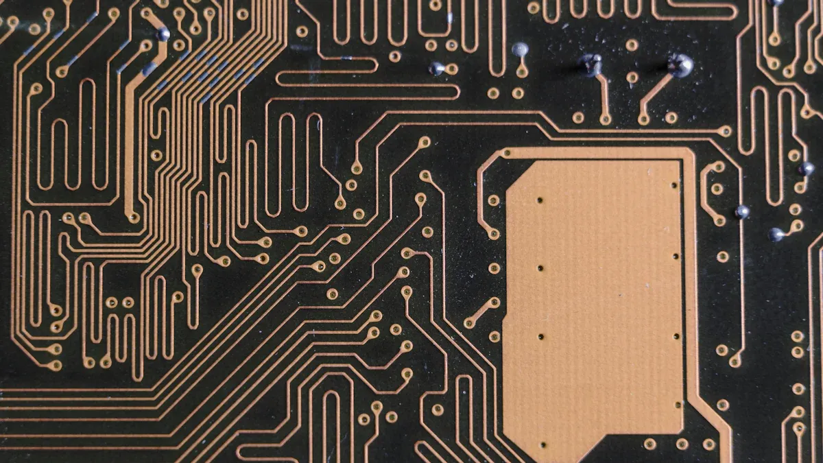
Solder mask bridges are thin parts of the solder mask. They separate nearby pads or pins on circuit boards. Their main job is to stop unwanted electrical connections. The solder mask is a plastic-like layer that protects the board. It makes sure solder sticks only to the right spots, avoiding mistakes.
These bridges are very important in crowded PCB designs. Without them, solder might spread between pads and cause problems. This problem, called solder bridging, happens when spacing is too small or designs are off. Adding solder mask bridges helps avoid these issues and keeps the PCB working well.
The role of solder mask bridges in preventing short circuits
Solder mask bridges help stop short circuits from happening. During soldering, melted solder can spread too far. If the solder mask is missing or not done right, it can connect nearby pads or pins. These unwanted connections, called solder bridges, can break devices.
The solder mask blocks solder from going where it shouldn’t. This is super important for tiny parts with little space between pads. By stopping solder from crossing gaps, solder mask bridges make PCBs more reliable and protect the parts.
Why solder mask bridges are critical for PCB reliability
PCBs work best when the solder mask does its job well. Solder mask bridges make sure connections happen only where they should. This lowers the chance of mistakes. If bridges are missing or poorly made, solder bridging can ruin the PCB.
Besides stopping short circuits, solder mask bridges shield the PCB from things like water and dirt. They also make the board last longer by reducing damage over time. For makers, good solder mask bridges are key to building strong, dependable PCBs that meet high standards.
Challenges of traditional solder mask application methods
Problems with old photolithography methods
Old photolithography is often used for solder mask application. But it has many problems that affect accuracy and efficiency. This method uses light and a mask to create patterns. It struggles to stay accurate, especially for crowded designs. Below is a table showing the main problems with photolithography:
Problem | Explanation |
|---|---|
Even light needed | Needs even light across the whole wafer, hard for big wafers. |
Perfect mask placement | Mask must align perfectly with features, making it tricky. |
Damage from touching | Touching can harm the mask and wafer, so it’s avoided in big production. |
Super clean workspace | Needs very clean areas, which are hard to keep. |
Flat surface only | Can’t work on surfaces that aren’t flat, limiting its use. |
These problems make photolithography less useful for today’s PCBs needing tiny solder mask bridges.
Problems with clarity, alignment, and shape
Old solder mask methods often have issues with clarity, alignment, and shape. Misalignment can leave copper pads exposed or unprotected, causing short circuits. Uneven layers are another problem, especially for small traces, hurting performance. Also, chemical reactions between the solder mask and some finishes, like OSP, can cause curing issues. These problems make PCBs less reliable and weaken the solder mask’s job.
Why old methods can’t make small solder mask bridges
Old methods can’t make small solder mask bridges because of their limits. They don’t control light and alignment well, leading to bigger gaps in patterns. This makes it hard to create narrow bridges needed for crowded PCB designs. Uneven layers and shape changes during curing also lower accuracy. This makes it tough to meet the needs of modern electronics.
How solder mask LDI works
Explaining the laser direct imaging process
Laser direct imaging (LDI) is a modern way to apply solder masks. It uses a laser beam instead of physical masks, making it more accurate. This method avoids errors and improves precision in PCB production.
First, a liquid solder mask is spread on the PCB. This layer reacts to light from the laser. The laser, guided by digital designs, shines on specific areas. This light changes the solder mask's properties. Parts not hit by the laser are washed away, leaving the pattern. Finally, the board is baked to harden the solder mask.
Here’s a simple breakdown of the LDI process:
Step | What Happens |
|---|---|
LPI coating | A liquid solder mask is applied, forming a sensitive layer. |
Imaging | A laser scans the board, exposing the design areas. |
Developing | Unwanted solder mask is removed, leaving the pattern. |
Curing (drying) | The solder mask is dried to stick firmly to the board. |
Final baking | The board is baked to harden the solder mask completely. |
This method ensures accuracy and works well for modern PCB designs.
Main features of solder mask LDI technology
LDI technology has special features that make it better than older methods. These features are great for complex and crowded PCB designs:
Feature | What It Means |
|---|---|
High Resolution and Precision | LDI can create very fine lines, perfect for small designs. |
Design Flexibility | Changes can be made quickly without needing new physical masks. |
Fewer Processing Steps | The process is simpler, reducing mistakes and saving time. |
Better Yield and Consistency | More accurate results mean stronger and more reliable PCBs. |
These features show why LDI is a top choice for PCB manufacturing. It makes creating detailed designs easier and faster.
Why LDI gives better precision and control
LDI offers excellent control when applying solder masks. The laser, guided by computer designs, ensures every detail is perfect. This reduces mistakes like misalignment or distortion.
The process includes these steps for better accuracy:
Design graphics: Circuit patterns are made using special software.
Generate images: Designs are turned into digital files for the laser.
Laser scanning: The laser follows the digital design to expose the solder mask.
Photochemical reaction: The solder mask reacts to the laser, changing its properties.
Development: Unexposed parts are removed, leaving the pattern.
Etching or electroplating: Extra steps finalize the circuit.
Without physical masks, LDI avoids contamination and ensures consistent results. Advanced lasers allow for precise exposure, making smaller solder mask bridges possible. This supports high-density PCB designs.
Tip: LDI is perfect for tiny and detailed designs. It ensures accuracy and reliability for advanced PCBs.
Why solder mask LDI enables smaller solder mask bridges
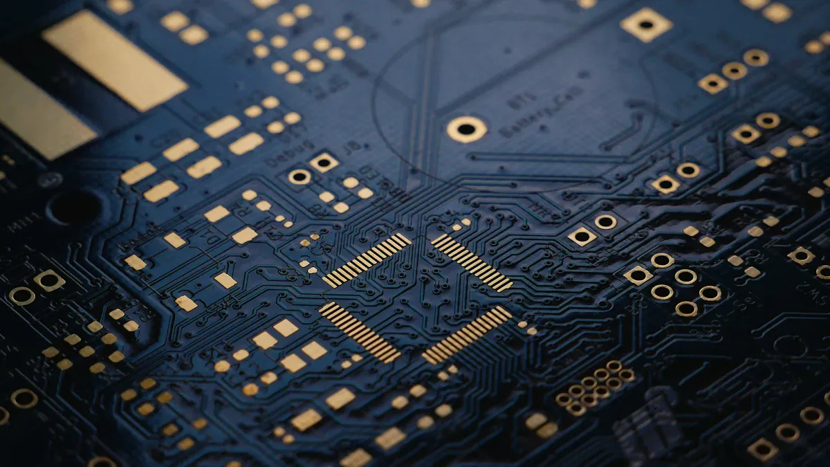
Better precision with laser direct imaging
Solder mask LDI uses lasers for very detailed patterns. These patterns are important for modern PCBs. Unlike old methods, LDI doesn’t need physical masks. It uses digital designs to guide the laser. This makes sure every part is accurate. With this control, smaller solder mask bridges can be made without losing quality.
LDI’s high resolution covers even tiny gaps between solder pads. This stops solder from spreading to wrong areas. For crowded PCBs, this accuracy is very important. LDI helps make PCBs for advanced devices like smartphones and IoT gadgets.
Note: LDI is great for small devices like smartwatches and medical tools.
Fixing alignment and shape problems
Old solder mask methods often have alignment problems. Misaligned layers can leave copper pads exposed. This can cause short circuits or make PCBs less reliable. LDI solves this by using lasers that match digital designs perfectly. This ensures each solder mask layer is applied correctly.
Distortion is another problem with old methods. Shapes and thickness can change during curing. LDI uses advanced lasers to avoid this issue. It keeps solder mask layers even and consistent. This makes PCBs more reliable and longer-lasting.
By fixing alignment and distortion issues, LDI improves solder mask quality. This helps PCBs work better and last longer.
Helping with high-density PCB designs at LT CIRCUIT
High-density PCBs need special techniques to handle their challenges. LT CIRCUIT uses LDI to meet these needs. LDI creates tiny traces and microvias for HDI PCBs. These features are key for compact and efficient designs.
Here’s how LT CIRCUIT supports high-density PCBs:
LDI makes very fine traces for small devices like wearables.
Microvias help create compact designs for HDI PCBs.
LDI speeds up prototyping, making design changes faster.
With LDI, LT CIRCUIT makes high-quality PCBs for advanced technology. Whether for consumer gadgets or industrial tools, their LDI expertise ensures precise and reliable results.
Benefits of smaller solder mask bridges in PCB manufacturing
Improved PCB performance and reliability
Smaller solder mask bridges make PCBs work better and last longer. They keep solder pads apart, stopping solder from connecting wrongly. This helps electrical connections stay strong in crowded designs. Smaller bridges also improve solder joints, making them rounder and stronger. These joints boost both strength and conductivity.
Here’s a comparison of smaller and larger solder mask bridges:
Aspect | Smaller Pads | Larger Pads |
|---|---|---|
Reliability | Better reliability with stronger joints | Lower reliability with higher solder bridging risk |
Yield | Lower yield | Higher yield |
Joint Shape | Rounder solder joints | Less round solder joints |
Routing Space | More space for circuits | Less space for circuits |
Smaller bridges make PCBs more reliable over time, especially for tough uses.
Helping miniaturization and advanced designs
Smaller solder mask bridges are important for tiny and advanced PCBs. They allow tighter spaces and smaller features, perfect for compact devices. Technologies like SiP and HDI need smaller bridges to fit more parts in small areas. Flexible PCBs also use smaller bridges to meet strict size limits while working well.
Trends pushing smaller solder mask bridges include:
SiP packaging makes assembly easier and faster.
Flexible PCBs need precise sizes and electrical values.
Microcircuits require tiny spaces for better performance.
These trends make smaller solder mask bridges essential for modern gadgets like wearables and medical tools.
Saving money in high-density PCB production
Smaller solder mask bridges help save money in PCB making. LDI technology skips photomasks, cutting material costs and waste. It also speeds up production, making it quicker and more flexible. While LDI systems cost more upfront, they save money over time, especially for prototypes and small batches.
Extra benefits of LDI include:
Less harm to the environment with fewer chemicals and waste.
Better energy use compared to older methods.
By simplifying the process and reducing waste, smaller solder mask bridges help manufacturers save money on high-density PCB designs.
Solder mask LDI is changing how PCBs are made. It helps create smaller solder mask bridges with great accuracy. This meets the needs of tiny electronics. More companies now want high-resolution tools for making detailed PCBs. LT CIRCUIT uses this advanced method to make strong and reliable PCBs. By skipping photomasks, LDI saves time and supports eco-friendly practices. This technology keeps you ahead in the fast-moving electronics world.
Did you know? In 2021, the U.S. PCB industry was worth $15.5 billion. This shows how important LDI is for modern electronics.
FAQ
What is the smallest solder mask bridge size possible with LDI?
With LDI, solder mask bridges can be as small as 3W. This high precision works well for dense PCB designs. It’s perfect for advanced devices like smartphones and wearables.
How does LDI make PCB manufacturing faster?
LDI removes the need for physical photomasks. This cuts down steps, reduces mistakes, and speeds up production. It also allows quick changes for prototypes or small orders.
Can LDI be used for all PCB types?
Yes, LDI is great for many PCB types, like HDI and flexible ones. Its accuracy and adaptability make it ideal for small, high-tech devices like medical tools and IoT gadgets.
Tip: Use LDI in your next PCB project for better precision and dependability.
See Also
How LDI Technology Affects PCB Product Quality
Advantages of LDI Machines in HDI PCB Circuit Production
Utilizing Horizontal Copper Sinking Technology in PCB Manufacturing