Step by Step Guide to Making a 2 Layer Aluminum PCB
You can make a 2 layer aluminum pcb by following a series of clear steps. Start with your design, select quality aluminum, and focus on thermal management for reliable performance. Many 2 layer aluminum pcb boards handle heat well, making them popular in high-power and heat-sensitive uses. For example, you often find 2 layer aluminum pcb in power amplifiers, LED lighting, and outdoor electronics.
Application Type | Specific Use Cases |
|---|---|
High-power applications | Power amplifiers, automotive circuits |
Outdoor or humid environments | Industrial lighting, marine electronics |
Cost-effective, high-thermal uses | LED lighting, heat-sensitive electronics |
Careful planning helps you avoid common mistakes and ensures your 2 layer aluminum pcb works as intended.
Key Takeaways
Start with a strong design to avoid mistakes. Plan both copper layers carefully for efficient signal routing.
Choose high-quality materials for better heat dissipation. Select the right aluminum alloy and dielectric layer based on your project needs.
Focus on thermal management during design. Use thermal interface materials and optimize spacing to enhance heat dissipation.
2 Layer Aluminum PCB Basics
Structure and Layers
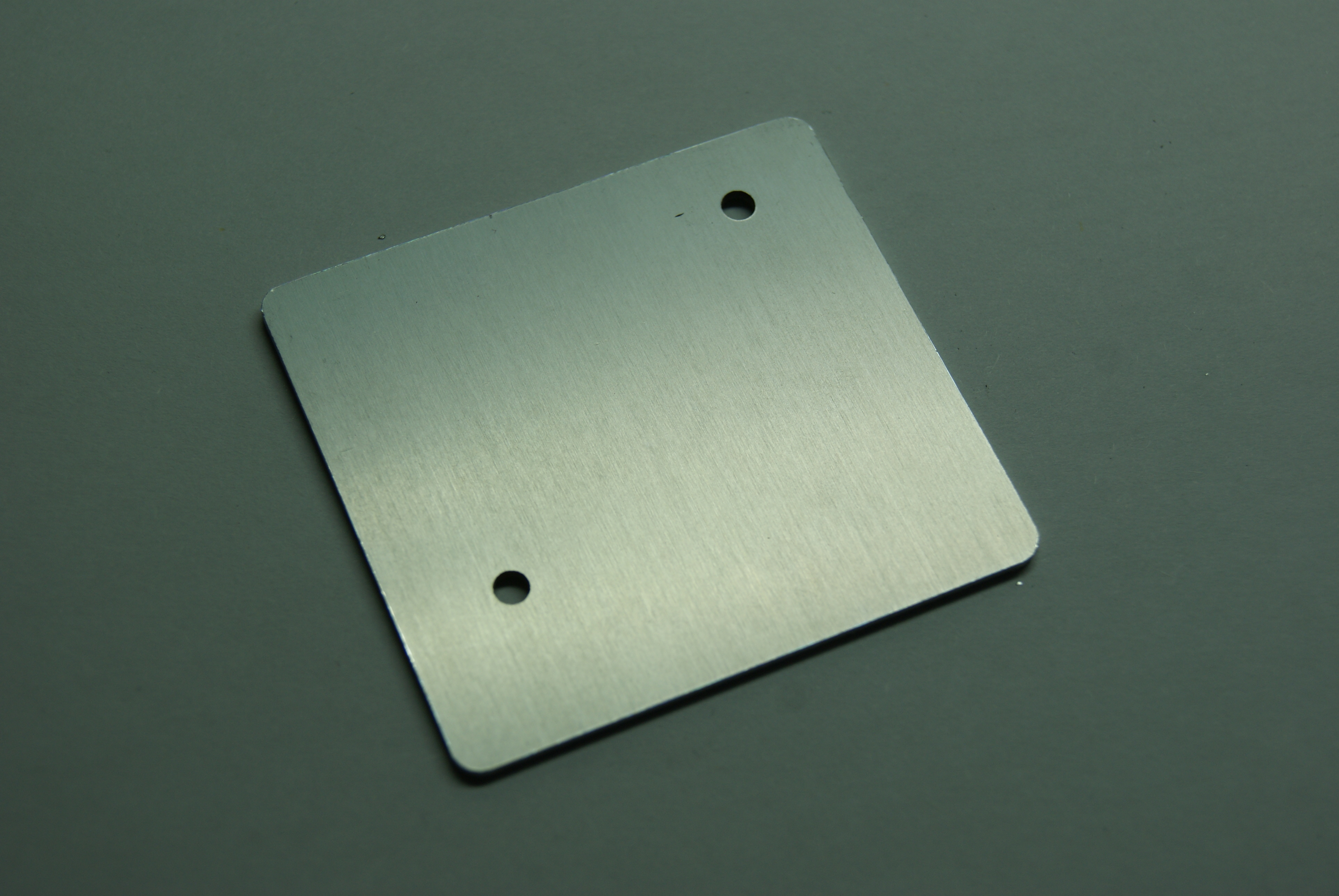
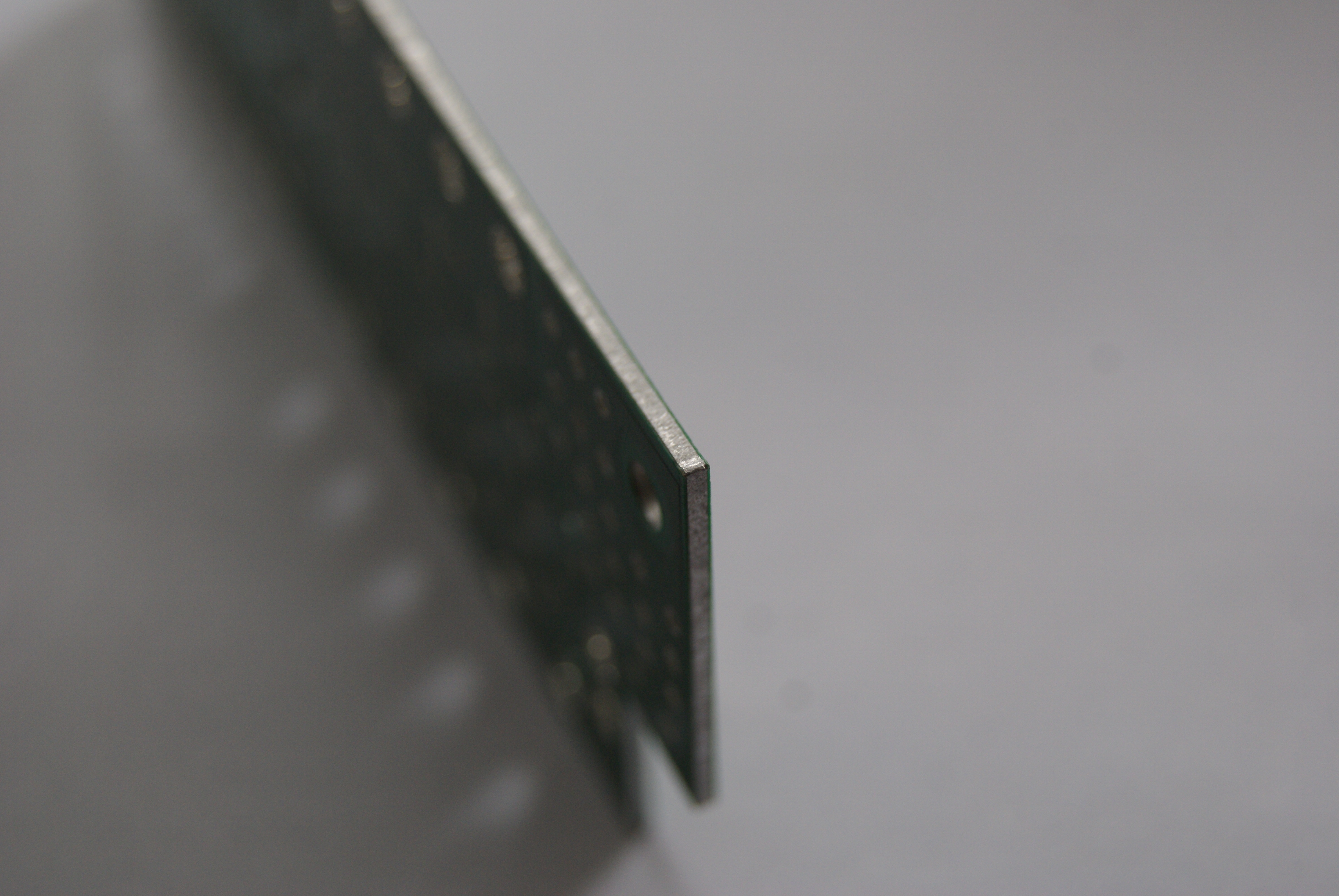
When you look at a 2 layer aluminum pcb, you see a unique structure that supports both electrical and thermal needs. This type of aluminum pcb uses two copper layers, separated by a dielectric layer, all mounted on a sturdy aluminum base. The metal substrate gives the board strength and helps with heat dissipation. Here is a table comparing single and 2 layer aluminum pcb structures:
Feature | Single Layer PCB | 2 Layer PCB |
|---|---|---|
Copper Layers | Present | Present |
Dielectric Heat Sink Layer | Present | Present |
Metal Substrate | Aluminum base (0.8-3.0mm thick) | Aluminum base (0.8-3.0mm thick) |
Thermal Conductivity | Options of 1/1.5/2W/mK | Options of 1/1.5/2W/mK |
Tensile Strength | Surpassing 200MPa | Surpassing 200MPa |
Temperature Resistance | Up to 200°C | Up to 200°C |
Resistance to Bending | Yes | Yes |
Corrosion Resistance | Yes | Yes |
Key Materials and Properties
You will find that aluminum pcb boards use specific materials for each layer. The copper foil acts as the main conductor. The dielectric layer sits between the copper and the aluminum, providing electrical insulation and helping with heat transfer. The aluminum base supports the structure and boosts heat dissipation. Here is a quick look at the typical materials:
Layer Type | Material Description |
|---|---|
Dielectric Layer | Thermally conductive but electrically insulating material |
Conductive Layer | Copper foil |
The overall thickness of a standard 2 layer aluminum pcb is about 1.6±0.1mm, using Aluminum 3001 and 2OZ copper. Aluminum offers thermal conductivity from 1W/mK to 9W/mK and can handle temperatures up to 400℃. This makes aluminum-based pcb boards ideal for high-power uses.
Thermal Management Considerations
You need to focus on thermal management when you design an aluminum pcb. Aluminum has excellent heat dissipation, which is why it is popular in high-power electronics. The metal core acts as a heat spreader, moving heat away from sensitive parts. Aluminum pcb boards have thermal conductivity about 600 times higher than FR4 boards, so they provide excellent heat dissipation. For best results, use thermal interface materials like pads or grease, and keep spacing at least 0.2 mm to allow for expansion. Good design choices help you get the most out of your aluminum pcb and keep your devices cool.
2 Layer Aluminum PCB Manufacturing Steps
Design and Layout for 2 Layer PCB
You start the manufacturing process by focusing on the design. A strong design helps you avoid costly mistakes later. For a 2 layer aluminum pcb, you need to plan both the top and bottom copper layers. This double sided pcb structure lets you route signals and power efficiently. Use industry-standard software tools to create your circuit design. Here is a comparison of popular options:
Software Tool | Features |
|---|---|
Altium Designer | Customizes circuit boards, supports metal substrate, smart placement, and rules checking. |
PCB Artist | User-friendly, helps you create accurate designs quickly. |
Target 3001 | All-in-one tool for professional layouts and designs. |
Siemens Solid Edge | Offers libraries, automated placement, and efficient design management. |
When you design a two-layer aluminum pcb, pay attention to these layout tips:
Map power and model heat flow to spot hot areas.
Choose trace widths that reduce heat buildup and signal loss.
Add thermal vias to move heat from hot parts to the aluminum base.
Optimize the stack-up to improve heat dissipation.
Plan for airflow and use heat sinks if needed.
Tip: Good design choices at this stage make the rest of the manufacturing process smoother and help your aluminum pcb last longer.
Material Selection and Preparation
Choosing the right materials is key for a reliable two-layer aluminum pcb. You need to select the aluminum alloy and dielectric layer based on your project’s needs. Here is a quick guide:
Material Type | Criteria |
|---|---|
Aluminum Alloys | 6061, 5052, 1060 for heat transfer, strength, and corrosion resistance |
Dielectric Layer | Thickness between 75µm to 200µm for thermal performance |
Cut the aluminum and copper foil to size before you start manufacturing. Make sure you use high-quality aluminum to get the best heat dissipation and mechanical strength. If you use poor materials, your 2 layer pcb may fail under stress or heat.
Aluminum PCB Stack-Up Design
The stack-up design affects both the mechanical and thermal performance of your 2 layer aluminum pcb. You arrange the layers to create low-resistance paths for heat to move from components to the metal substrate. This helps with heat dissipation and keeps your double sided pcb cool.
Layer | Configuration Description |
|---|---|
Top | Signal and power traces, ground pour to reduce impedance. |
Bottom | Dedicated to ground. |
Both | Ground pours on both layers, connected with vias for better signal integrity. |
A balanced stack-up improves electrical performance and mechanical strength. Work closely with your manufacturer to get the best results for your aluminum pcb.
The stack-up design impacts electrical, thermal, and mechanical properties.
Proper arrangement of layers and components is crucial for performance.
Dielectric and Surface Preparation
Before you start building your two-layer aluminum pcb, you need to prepare the aluminum surface. This step improves adhesion and reliability. You can use physical grinding or chemical etching to roughen the surface. Alkali etching works best for creating a micro-rough surface that helps the dielectric layer stick to the aluminum.
Note: Too much roughness can hurt adhesion, so aim for a balanced surface.
Standard preparation steps include:
Select and cut the aluminum and copper foil.
Treat the surface to improve adhesion and corrosion resistance.
Laminate the copper foil onto the aluminum base.
This careful preparation ensures your 2 layer pcb will handle heat and stress during use.
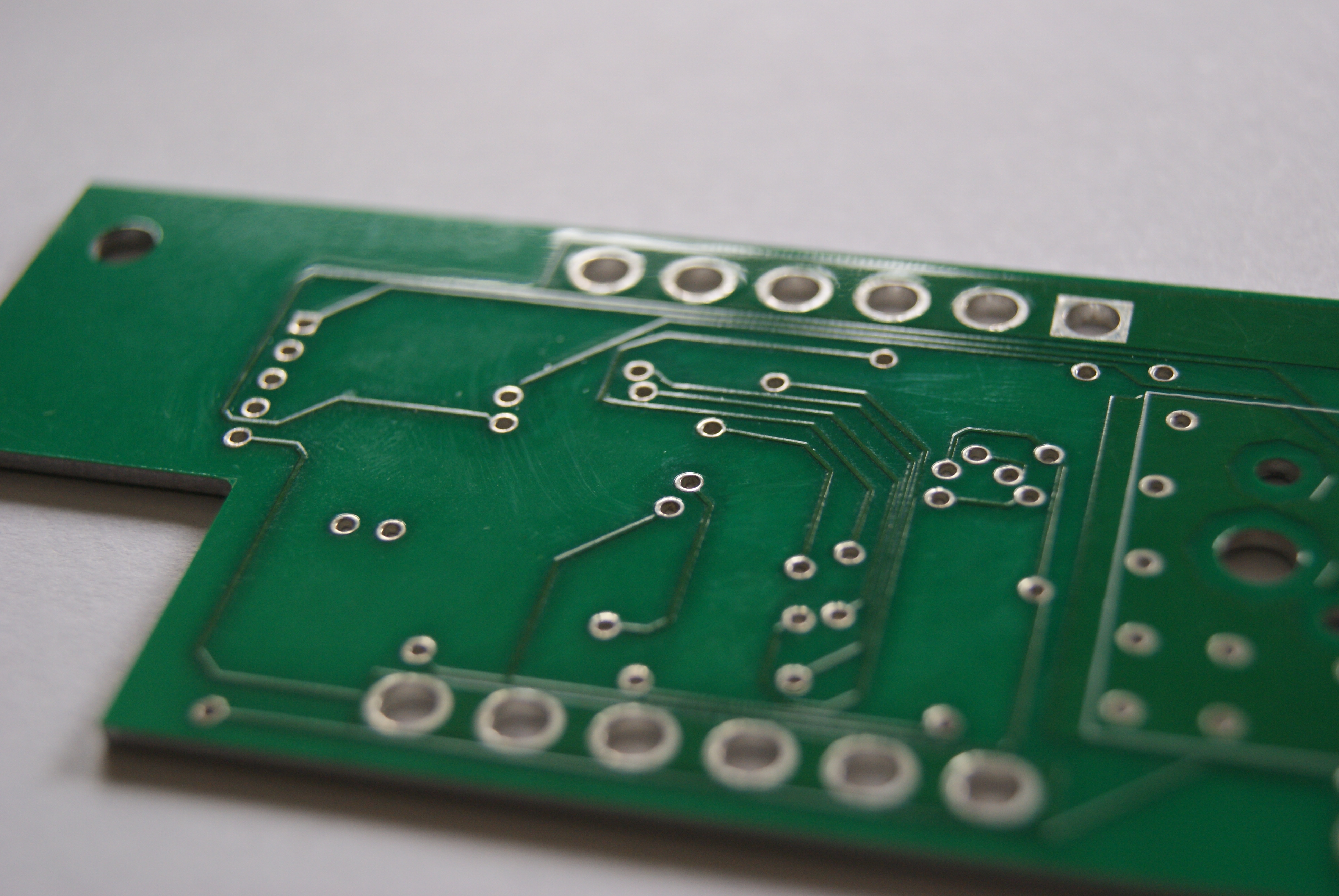
Circuit Patterning and Etching
Now you create the circuit paths on your aluminum pcb. Start by applying a photosensitive film to the copper. Use light to transfer your circuit design onto the film. Next, use chemical etching to remove unwanted copper, leaving only the desired traces.
Common defects during etching include:
Defect Type | Symptoms | Solutions |
|---|---|---|
Excessive Side Etching | Burrs, line width deviation | Add glycerol, adjust spray pressure, use pulsating etching |
Aluminum Surface Corrosion | Deep etch pits | Control pH, use dual-layer photoresist, citric acid neutralization |
Fine Line Breakage | Discontinuities in traces | Use ultra-low profile copper, optimize pre-bake, slow etching |
Uneven Etching | Copper thickness variation | Use rotating rack, optimize nozzle layout, monitor thickness |
Residual Copper Slag | Copper particles between traces | Use ultrasonic cleaning with deionized water |
Tip: Monitor the etching process closely to avoid defects that can weaken your double sided pcb.
Drilling and Via Formation
Drilling creates the holes and vias that connect the two layers of your 2 layer pcb. You can use mechanical drilling for larger holes or laser drilling for smaller, more precise vias. Here is a summary:
Drilling Technique | Description | Hole Size Capability |
|---|---|---|
Mechanical Drilling | Uses drill bits, less precise, easy to use | Minimum 6 mil |
Laser Drilling | Non-contact, very precise, for small holes | Minimum 2 mil |
Blind and Buried Vias | Drilled before lamination, controlled depth | Varies |
Micro-vias | Laser-drilled, ideal for thick PCBs | Very small sizes |
Through-hole vias connect both layers, while blind and buried vias connect only some layers. Micro-vias work well for thick aluminum-based pcb boards.
A two-layer aluminum pcb offers better heat dissipation and reliability than traditional FR4 boards. The aluminum base keeps components cool and improves the safe operating temperature.
Plating and DBC Application
After drilling, you need to plate the holes and apply direct bonded copper (DBC) if your design requires it. Plating improves conductivity and corrosion resistance. DBC substrates use a thick copper layer bonded to a ceramic base, such as aluminum oxide or aluminum nitride, through high-temperature diffusion. This process gives your aluminum pcb excellent thermal conductivity and electrical insulation.
Pre-oxidize the copper foil.
Stack and laminate the copper on the ceramic layer.
Bond at high temperature in a nitrogen or hydrogen atmosphere.
Cool to ensure a strong, void-free interface.
You find DBC in high-power uses like automotive, industrial, and renewable energy systems.
Solder Mask and Silkscreen
Apply a solder mask to protect the copper traces and prevent short circuits during assembly. Next, print the silkscreen to add labels and component positions. You may face challenges with adhesion because aluminum has a smooth surface. Make sure the dielectric layer bonds well to the aluminum to avoid problems.
Thermal stress can cause expansion and stress at solder joints. Use high-quality materials and control the manufacturing process to reduce these risks. Sourcing good aluminum and dielectric materials can be tough, so plan ahead.
Surface Finish and Testing
Finish the surface to improve solderability and protect the copper. Common finishes include HASL, ENIG, and OSP. After finishing, test your 2 layer aluminum pcb to ensure quality.
Testing Method | Description |
|---|---|
Solderability Testing | Checks solder joint strength and durability. |
Cleanliness Testing | Measures contamination to prevent corrosion. |
Reliability and Stress Testing | Simulates real-world conditions for long-term reliability. |
Electrical Performance Testing | Checks continuity and insulation resistance. |
Mechanical Performance Testing | Tests physical strength under stress. |
Environmental Adaptability Testing | Evaluates performance in different environments. |
Note: Always test for continuity and insulation resistance to catch any faults before assembly.
By following these steps, you can complete the manufacturing process for a high-quality two-layer aluminum pcb. Careful design, material selection, and attention to detail at each stage help you achieve strong heat dissipation and reliable performance in your aluminum pcb.
You can make a reliable aluminum pcb by following each step carefully. Start with a checklist:
1. Layer stackup 2. Signal solidarity 3. Component placement 4. Routing 5. Ground plane 6. Power distribution 7. Thermal management 8. Manufacturing constraints 9. EMI/EMC compliance 10. Testability
Watch for common mistakes like incorrect Gerber files, BOM errors, solder paste issues, and copper balancing problems. Always check aluminum surface quality, thermal conductivity, and adhesion strength. Use thermal imaging and visual inspection to confirm heat dissipation. With patience and the right approach, you can achieve a high-quality aluminum pcb using aluminum for strong thermal performance.
FAQ
What makes a 2 layer aluminum PCB better for heat management?
You get better heat dissipation because the aluminum base spreads heat quickly. This keeps your components cooler and improves reliability.
Can you solder components directly onto an aluminum PCB?
You should not solder directly onto the aluminum. Always solder to the copper pads. The dielectric layer insulates the copper from the aluminum base.
How do you test a finished 2 layer aluminum PCB?
You can use a multimeter to check for continuity and shorts. Visual inspection helps you spot defects. Thermal imaging shows how well your board handles heat.
See Also
Understanding The Comprehensive Process Of Multilayer PCB Production
Challenges In Prototyping And Manufacturing Multilayer Circuit Boards
An In-Depth Look At The PCB Fabrication Process