Step-by-step process for creating multilayer PCBs for RFID systems

You need a reliable approach when you design a multilayer rfid pcb. Power and ground planes help you control noise. You improve signal integrity with careful layer planning. Antenna integration lets your system read tags accurately.
Key Takeaways
Define system requirements early. Choose the right frequency band and board size for your RFID application to ensure optimal performance.
Plan your PCB layout carefully. Place antennas away from noise sources and ensure a solid ground plane to enhance signal integrity.
Follow best practices in schematic preparation. Use standard file formats and maintain proper spacing between components to avoid manufacturing issues.
Multilayer RFID PCB Design
System Requirements
You start your multilayer rfid pcb project by defining system requirements. The operating frequency and size of your circuit board shape the entire design. RFID applications use different frequency bands, each with its own range and performance. You can see the standard frequency bands in the table below:
Frequency Band | Frequency Range |
|---|---|
Low Frequency (LF) | 125kHz to 134.2kHz |
High Frequency (HF) | 13.56MHz |
Ultra-High Frequency (UHF) | 860MHz to 960MHz |
Microwave | 2.45GHz |
You select the frequency band based on your application. For example, UHF works well for long-range tracking, while HF suits secure access cards. The size of your circuit board also matters. Smaller boards fit compact devices, but you must balance size with antenna performance.
When you plan your circuit board design, you need to decide where to place the RFID chip and antenna. The table below shows key requirements for placement:
Requirement | Description |
|---|---|
PCB Layout Design | The layout must consider the placement and orientation of the chip antenna. |
Ground Plane Size | The size of the ground plane is critical for the radiation properties of the chip antenna. |
Clearance from Components | Antennas should be placed away from noise-generating components to minimize interference. |
Avoid Overlapping Ground Planes | In multilayer PCBs, overlapping ground planes can interfere with signal propagation. |
Tip: Place antennas at the edge of the circuit board and keep them away from power ICs, clocks, and signal buses. Always check the antenna’s data sheet for recommended clearances.
A solid ground plane helps your antenna work better. For short-range applications, you can use a smaller ground plane. For longer ranges, you need a larger ground plane to boost performance.
Schematic and File Prep
You create a schematic to show how every part connects on your multilayer rfid pcb. This step lets you plan the circuit board design and avoid mistakes later. You use standard file formats to share your design with manufacturers. The most common formats include DXF and DWG, which define the board shape and come from CAD software like SolidWorks.
File Format | Description |
|---|---|
DXF/DWG | Used for defining board shape from mechanical designs, can be exported from CAD software like SolidWorks or GeoMagic. |
Multi-layer PCBs often start with a 4-layer configuration. You use two internal power planes and two outer signal layers. This setup supports complex routing and improves signal integrity.
When you prepare your design files, you follow best practices to ensure manufacturability:
Keep enough space between components for automated placement and rework.
Use trace widths and spacings that match manufacturer standards and support required current loads.
Choose standard via sizes and make sure annular rings are large enough for reliable connections.
Specify solder mask clearances to prevent solder bridging.
Work with your PCB fabricator early to spot and fix manufacturability issues.
You check every detail in your schematic and layout before sending files to the manufacturer. Careful preparation helps you avoid costly errors and delays.
Stackup and Layer Planning
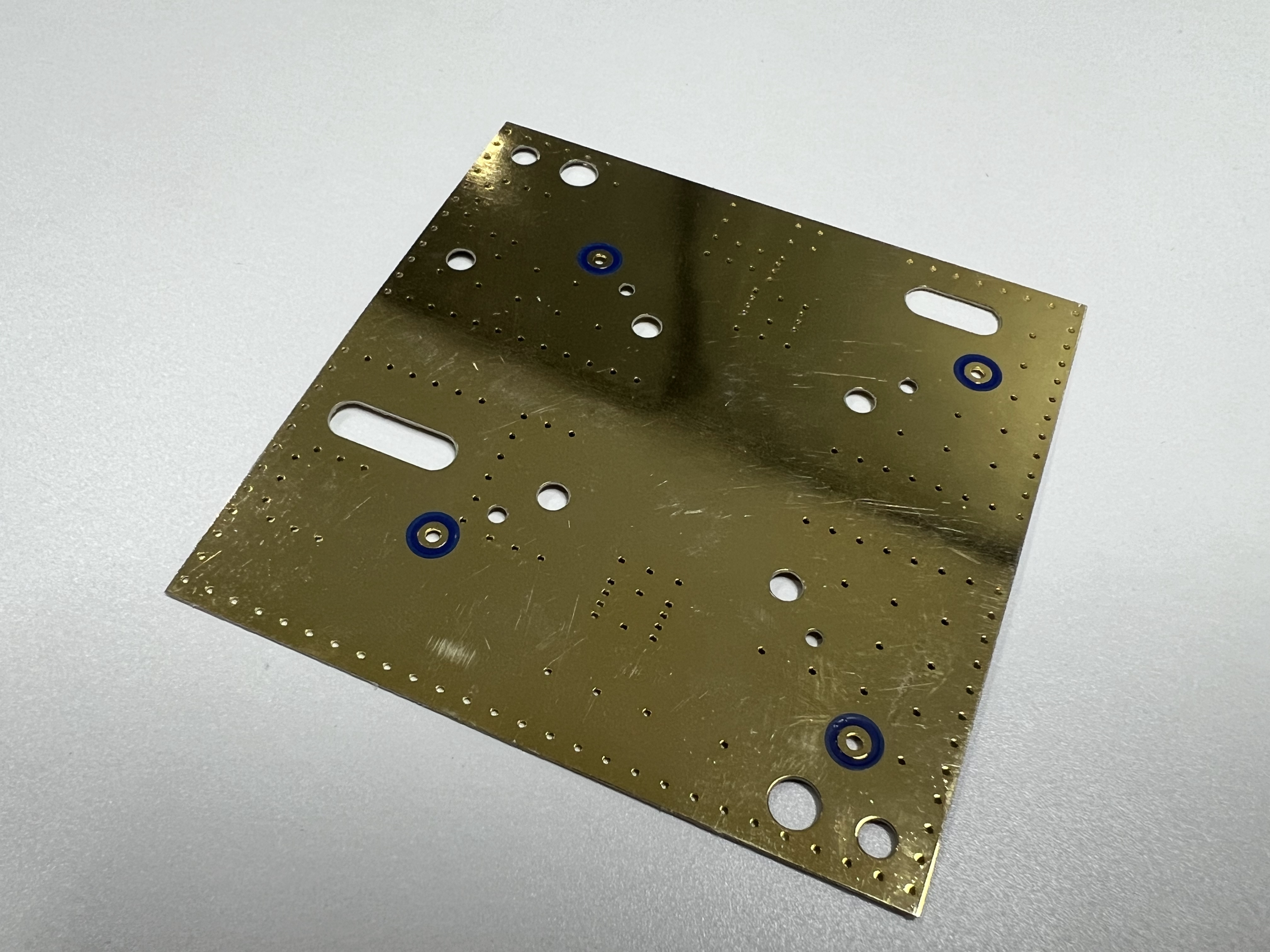
You plan the layer stack-up configuration to optimize signal integrity and minimize electromagnetic interference (EMI). The stackup defines how you arrange signal, power, and ground layers in your multilayer rfid pcb. You choose the number of layers based on your application and routing needs.
Description | |
|---|---|
8 Layers | Improves EMC performance with two additional planes; limits adjacent signal layers to reduce impedance discontinuities and crosstalk. |
10 Layers | Ideal for six routing layers and four planes; provides tight coupling and shielding for high-speed signals. |
12 Layers | Suitable for high-speed requirements with excellent EMC performance; provides shielding on six internal layers. |
14 Layers | Used for eight routing layers with special shielding for critical nets; provides isolation for sensitive signals. |
16 Layers | Offers ten routing layers for dense designs; often used when routing technology is insufficient without adding layers. |
You use dedicated power and ground planes to control EMI. A solid, continuous ground plane gives your circuit board a low-impedance path for return currents. It acts as a shield and keeps electromagnetic fields contained. Tuning the power and ground planes protects your circuit board from interference and improves the integrity of high-frequency signals.
Note: Good stackup planning reduces noise and crosstalk. It also helps you maintain signal integrity for RFID applications.
You select the right number of layers and arrange them to support trace routing and isolation. This step is critical for reliable multilayer rf pcbs.
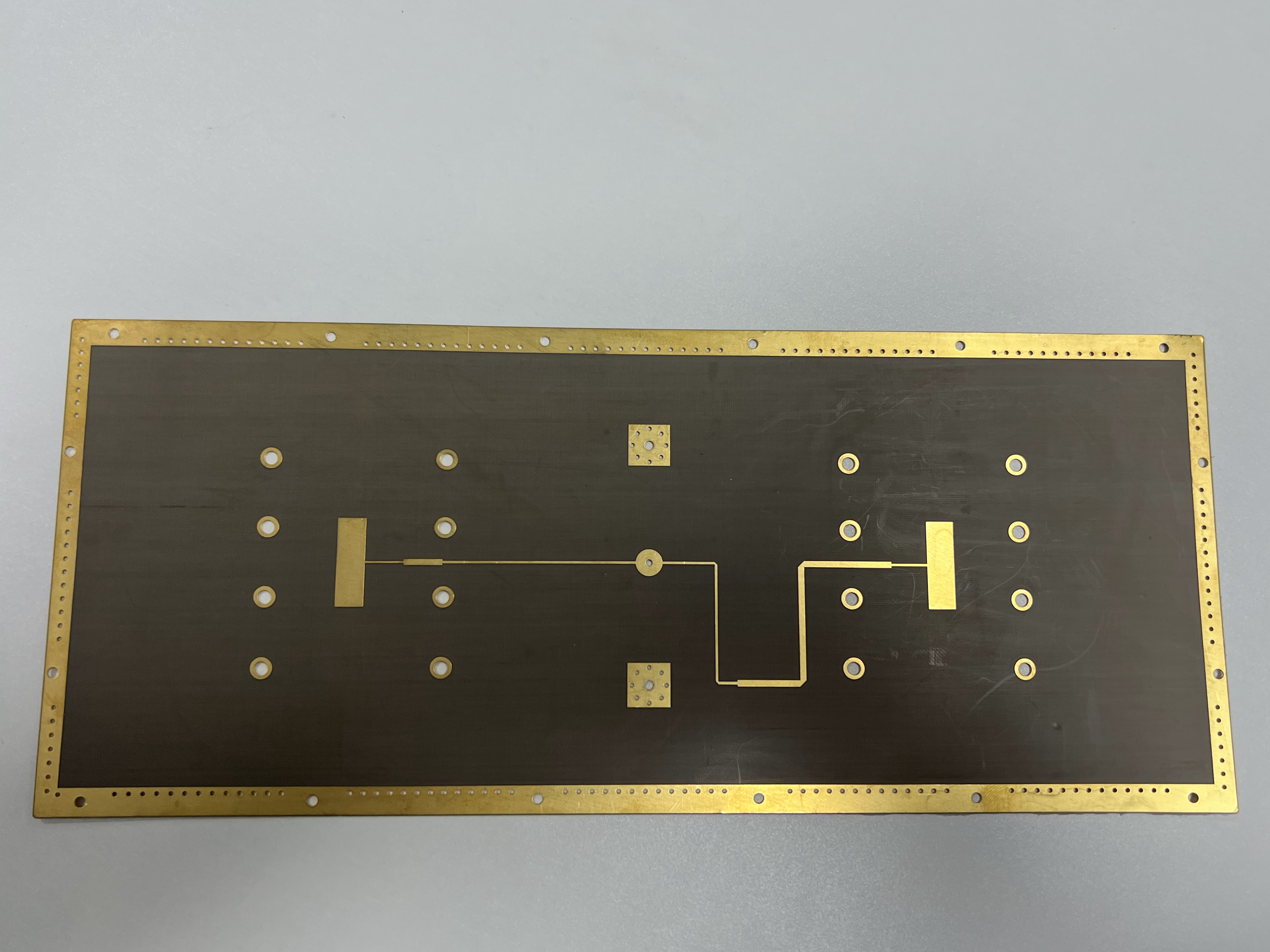
Antenna Integration
You integrate the antenna into your multilayer rfid pcb to enable tag reading and communication. You can use several methods to embed antennas in the circuit board. Some popular techniques include embedded RFID systems, the MAGIC-PCB technique, and Murata’s Magicstrap. These methods let you build antennas directly into the printed circuit boards or mount compact RFID components.
Method/Feature | Description |
|---|---|
Embedded RFID Systems | Integrates RFID directly into the PCB structure, allowing the PCB to function as an RFID tag. |
MAGIC-PCB Technique | Developed by Beta LAYOUT, enables embedding RFID in prototypes with specific antenna designs. |
Murata’s Magicstrap | A compact RFID component that can be embedded or surface mounted, utilizing smaller antenna designs. |
Adaptive Matching Circuit | Allows the PCB ground plane to act as an antenna, enhancing read distances and performance. |
Turnkey Antenna Designs | Provides ready-to-use antenna designs that can be integrated into existing PCB layouts. |
You use adaptive matching circuits to tune the antenna and ground plane for better performance. This approach improves read distances and accuracy. You can also use turnkey antenna designs to speed up development for RFID applications.
Performance metrics for antenna integration include impedance matching, frequency range, and environmental resistance. For example, you match the antenna to the chip impedance, usually around 14.6−j 316 Ω. You use multilayer ceramic capacitors (MLCCs) with values of 33–68 pF for RF applications. Short-circuited constructions help your antenna resist environmental factors like metal frames and glass substrates.
You focus on antenna placement, matching, and material properties to achieve reliable multilayer rf pcbs. Good integration ensures your circuit board reads tags accurately and works in different environments.
Multi-layer PCB Fabrication Steps
Inner Layer Processing
You begin the fabrication of multilayer rf pcbs by preparing the inner layers. This step sets the foundation for your circuit board design and ensures the integrity of high-frequency signals. Follow these steps for inner layer processing:
Clean and condition the copper clad laminate. This removes contaminants and prepares the surface for photoresist application.
Apply and cure liquid photoresist. The photoresist protects the copper during imaging and etching.
Expose the inner layers using phototools and UV light. This process transfers your circuit board design onto the copper.
Develop the exposed inner layers. Chemicals remove unprotected photoresist, revealing the pattern for your circuit board.
Etch away unwanted copper. Only the areas protected by photoresist remain, forming the traces and planes for your multilayer rf pcbs.
Strip the remaining photoresist and treat the copper surface. This prepares the layers for bonding during lamination.
You must pay attention to each step. Mistakes in inner layer processing can affect signal integrity and the performance of your multilayer circuit board.
Lamination and Alignment
You stack the processed inner layers with prepreg and core materials. Lamination bonds these layers together to form a solid multi-layer pcb. You need precise alignment to maintain the integrity of your circuit board design. Uniform pressure and accurate temperature control help you avoid defects.
Defect Description | Impact |
|---|---|
Image is exposed incorrectly | Causes size variations in features |
Poor dry film resist adhesion | Leads to nicks, cuts, or pinholes |
Copper is under-etched | Results in unwanted copper or shorts |
Copper is over-etched | Creates reduced feature sizes or cuts |
Proper alignment of layers
Uniform pressure distribution
Accurate temperature control
You must check for these defects during lamination. Good lamination and alignment protect the performance of high-frequency signals and maintain the integrity of your multilayer rf pcbs.
Drilling and Vias
You drill holes for vias and component leads after lamination. Vias connect different layers in your multi-layer pcb and support complex circuit board design. You choose via types based on your routing needs:
Blind vias preserve routing channels and do not create keepout zones on layers they do not penetrate. This allows efficient routing in your circuit board.
Buried vias minimize electromagnetic interference and help maintain controlled impedance. This is important for high-frequency signals and signal integrity.
Through-hole vias enable complex routing architectures and support intricate internal connections.
Blind vias reduce circuit board size and improve signal integrity. Signals routed through blind vias experience less noise. You simplify layout by allowing direct connections between inner layers.
Standard | Aspect Ratio Recommendation |
|---|---|
IPC-2226 | Defines HDI requirements and microvia specifications |
IPC-2141 | Provides signal integrity guidelines |
IPC-2251 | Provides signal integrity guidelines |
General | Standard PCB through-hole vias should have an aspect ratio ≤ 10:1 |
General | Microvias must have an aspect ratio of 1:1 or lower |
You follow these standards to ensure drilling accuracy and reliable connections in your multilayer rf pcbs.
Copper Plating and Finish
You plate the drilled holes with copper to create electrical connections between layers. The finish you choose affects the durability and signal performance of your circuit board. You select a finish based on your design considerations and application needs.
Finish Type | Pros | Cons |
|---|---|---|
Hot Air Solder Leveling (HASL) | Excellent solderability, cost-effective | Uneven surface, not for high-frequency signals |
Electroless Nickel Immersion Gold (ENIG) | Flat surface, corrosion resistance, good for high-frequency signals | More expensive, risk of 'black pad' syndrome |
Immersion Tin | Good solderability, flat surface | Short shelf life, not for multiple reflow cycles |
Immersion Silver | Excellent solderability, good for high-frequency signals | Prone to oxidation, higher cost |
Organic Solderability Preservative (OSP) | Flat surface, environmentally friendly | Limited shelf life, not for high-frequency signals |
ENIG and immersion silver finishes work well for multilayer rf pcbs that handle high-frequency signals. These finishes provide a flat surface and protect the integrity of your circuit board.
Solder Mask and Marking
You apply solder mask to protect copper traces and prevent solder bridges during assembly. You must ensure adequate solder mask expansion around pads and via openings. This step keeps your circuit board design reliable and prevents shorts.
Place silkscreen markings away from component pads. This helps you identify components and their polarity without interfering with placement.
Insufficient coverage exposes copper traces and leads to corrosion. You avoid this by controlling solder mask thickness and cleaning surfaces before application.
High solder mask expansion values can cause oversized openings. This leads to solder bridging and poor wetting during assembly.
The solder mask characteristics affect the performance of multilayer rf pcbs, especially in high-frequency applications.
Tip: Always check solder mask and marking placement before finalizing your circuit board design. Good practices here protect the integrity of your multilayer circuit board.
Final Testing for Multilayer RF PCBs
You test your multilayer rf pcbs to verify performance and reliability. You check for electrical continuity, shorts, and opens. You also test antenna performance and signal integrity. These tests confirm that your circuit board design meets RFID requirements.
Use impedance testing to ensure high-frequency signals travel correctly.
Measure antenna read distance and accuracy.
Inspect solder mask coverage and marking clarity.
You must complete these tests before deploying your circuit board. Reliable testing ensures your multilayer rf pcbs deliver strong performance in RFID systems.
You achieve reliable RFID performance by following each step with care. Focus on signal routing, power distribution, and heat dissipation. Use high-quality materials and optimize antenna placement.
Maintain controlled impedance and minimize crosstalk.
Test thoroughly and avoid poor layout or low-quality materials.
Resource/Tool | Description |
|---|---|
Step-by-step guide | |
Trace Width Calculator | Calculates trace widths for signal integrity |
PCB Artist Software | Assists with PCB design and layout |
FAQ
What makes multilayer PCBs important for RFID applications?
You use multilayer pcb designs to improve signal integrity. These designs help your circuit board reduce noise. Many applications need strong performance and reliable tag reading.
How do you choose the right circuit board stackup for RFID applications?
You select a stackup based on your circuit board size and frequency. Many applications require dedicated power and ground planes. This helps your pcb support high-frequency signals.
Can you integrate antennas directly into the circuit board for RFID applications?
You can embed antennas in your circuit board. This method works well for many applications. You improve performance and save space on your pcb.
See Also
Understanding The Comprehensive Process Of Multilayer PCB Production
Exploring The Manufacturing Steps For Rigid-Flex Circuit Boards
Challenges And Processes In Multi-Layer Circuit Board Production