Everything You Need to Know About Making Multilayer Ceramic PCBs
Producing a multilayer ceramic pcb involves many meticulous steps, requiring specialized equipment and constant monitoring. Some common challenges include:
Complex processes in manufacturing the multilayer ceramic pcb
Rigorous inspections to ensure top quality
Understanding each stage of the multilayer ceramic pcb production process is essential for optimal performance. LT CIRCUIT excels in delivering expertly crafted multilayer ceramic pcb solutions.
Key Takeaways
Multilayer ceramic PCBs use special materials and careful steps. These steps help make strong boards. The boards can handle heat and work in tough places.
Good design and careful making are important. Laser drilling and lining up layers the right way help a lot. This makes sure the multilayer ceramic PCBs work well and last long.
These PCBs are great for high-power and high-frequency jobs. They also work well in hard conditions. That is why they are good for cars, planes, and medical devices.
Multilayer Ceramic PCBs
Structure and Materials
Multilayer ceramic pcbs have a special layered design. These boards stack ceramic layers on top of each other. Each layer has its own circuit pattern. This setup helps make small and strong multilayer pcb solutions for modern electronics.
When you look at multilayer ceramic pcbs and FR4 pcbs, you see some big differences:
Multilayer ceramic pcbs are harder but break more easily than FR4 boards.
Ceramic pcb designs usually have fewer layers and simpler vias.
Making a multilayer ceramic pcb needs special steps like laser drilling and metallization.
FR4 multilayer pcb boards can make smaller traces and pitches more simply.
Choosing the right material for multilayer pcbs matters a lot. The table below lists common ceramic materials and what they are good for:
Material | Properties | Typical Applications |
|---|---|---|
Alumina (Al2O3) | Handles heat well, saves money, works in tough places | LED lighting, car parts |
Aluminum Nitride (AlN) | Gets rid of heat fast, keeps electricity from leaking | Inverters, power supplies |
Beryllium Oxide (BeO) | Moves heat very well, stops electricity from crossing, hard to use | High-current, microwave products |
Silicon Carbide (SiC) | Gets rid of heat fast, very strong | Aerospace, cars, power electronics |
Hybrid Ceramic | Mixes metal and ceramic for special needs | High-performance uses |
Key Benefits
Multilayer ceramic pcbs have many good points over regular printed circuit boards. They handle heat really well because ceramic materials like aluminum nitride and alumina move heat better than FR4. This makes multilayer ceramic pcbs great for high-power and high-frequency jobs.
Ceramic pcb bases also stop electricity from leaking. They keep signals clear and help prevent shorts. Multilayer ceramic pcb boards stay strong and do not bend or crack when they get hot.
You can see that multilayer ceramic pcbs mix high heat movement with strong electrical insulation. This makes them perfect for tough jobs like power electronics, RF circuits, and aerospace.
LT CIRCUIT is a leader in making advanced multilayer ceramic pcb solutions. You can count on their skill and new ideas for your hardest multilayer pcb projects.
PCB Manufacturing Process
Making multilayer ceramic pcbs takes many steps. Each step helps make strong printed circuit boards for new electronics. You must follow a careful plan so your multilayer pcb works well and lasts long. LT CIRCUIT uses special materials and careful ways to get great results.
Design Phase
You begin by thinking about what your project needs. Multilayer pcb design needs extra care because ceramic acts different from other boards. Here are some important things to think about for multilayer ceramic pcbs:
Pick ceramic materials like alumina or aluminum nitride for good heat movement and strong electrical insulation.
Plan how the layers stack to control impedance and stop crosstalk.
Put power and ground planes close together to lower electromagnetic interference.
Use conductive-filled vias, like tungsten, to connect layers and keep signals strong.
Make signal paths that avoid interference and keep signals clear.
Choose surface finishes like immersion gold or silver for better soldering and protection.
Add thermal vias and plan the stack-up to help heat move away.
Make sure the board is thick and stiff enough for your use.
Place vias near parts to lower inductance and help performance.
Check if your design is easy to make and add stress relief to stop warping.
Tip: Planning carefully in the design phase helps you avoid problems later when making the multilayer pcb.
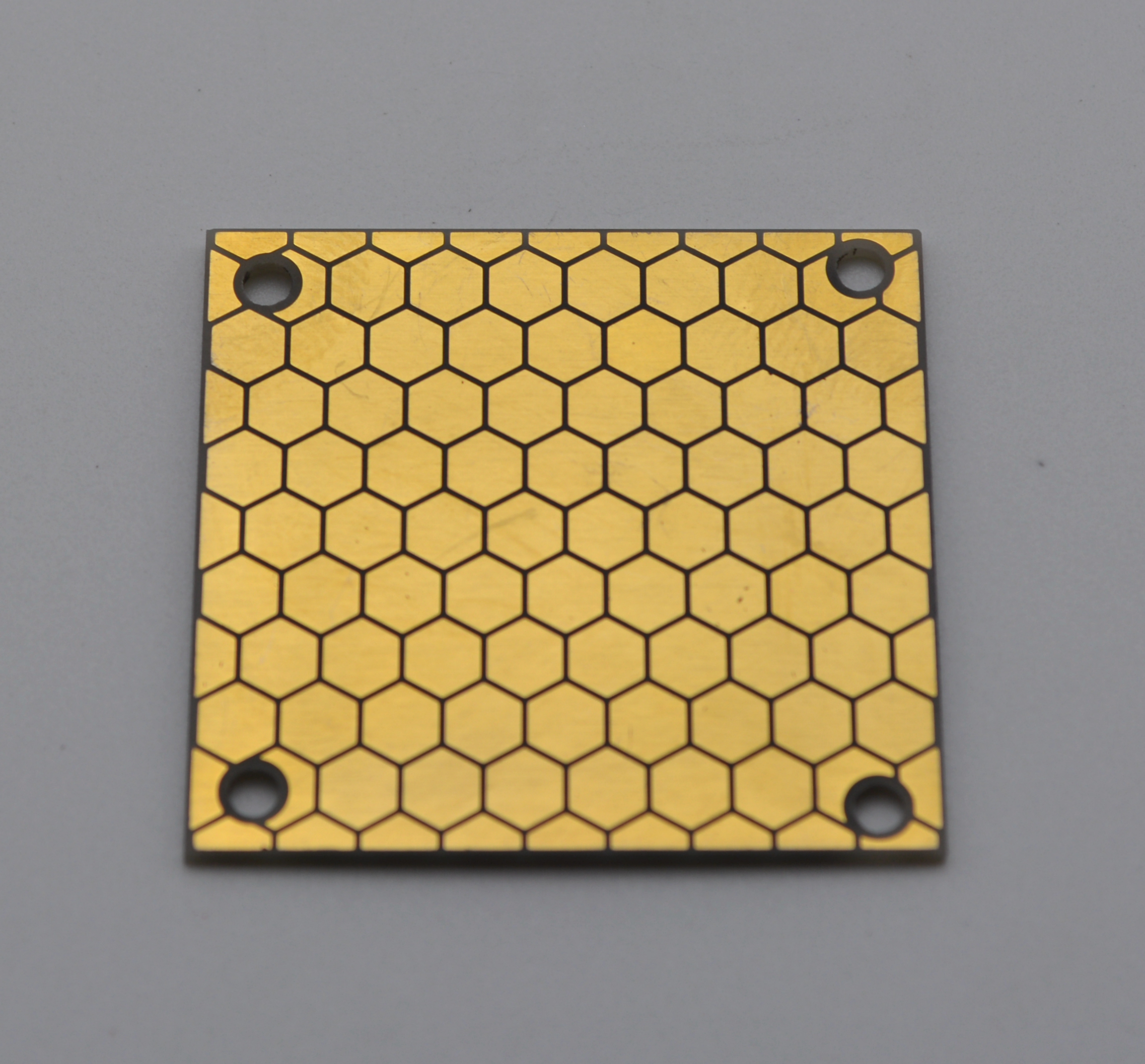
Substrate Preparation
Next, you get the ceramic base ready for building layers. LT CIRCUIT uses special ways to make sure each layer is clean and strong. Here is how you prepare the layers for multilayer pcbs:
Pick the right ceramic material, like alumina, aluminum nitride, or silicon carbide, for your needs.
Mix ceramic powders with binders and solvents to make a paste.
Use tape casting to make thin, even ceramic sheets called green sheets.
Clean and treat the surface of each sheet so layers stick together.
Print circuit patterns on the sheets using screen printing.
Stack and press the sheets to build the multilayer structure.
Drill or punch vias through the layers for electrical connections.
Cover the via walls with metal using electroplating or chemical vapor deposition.
Heat the stack at high temperatures to bond the layers and make the circuits work.
This careful work makes sure your multilayer pcb has strong layers and good connections.
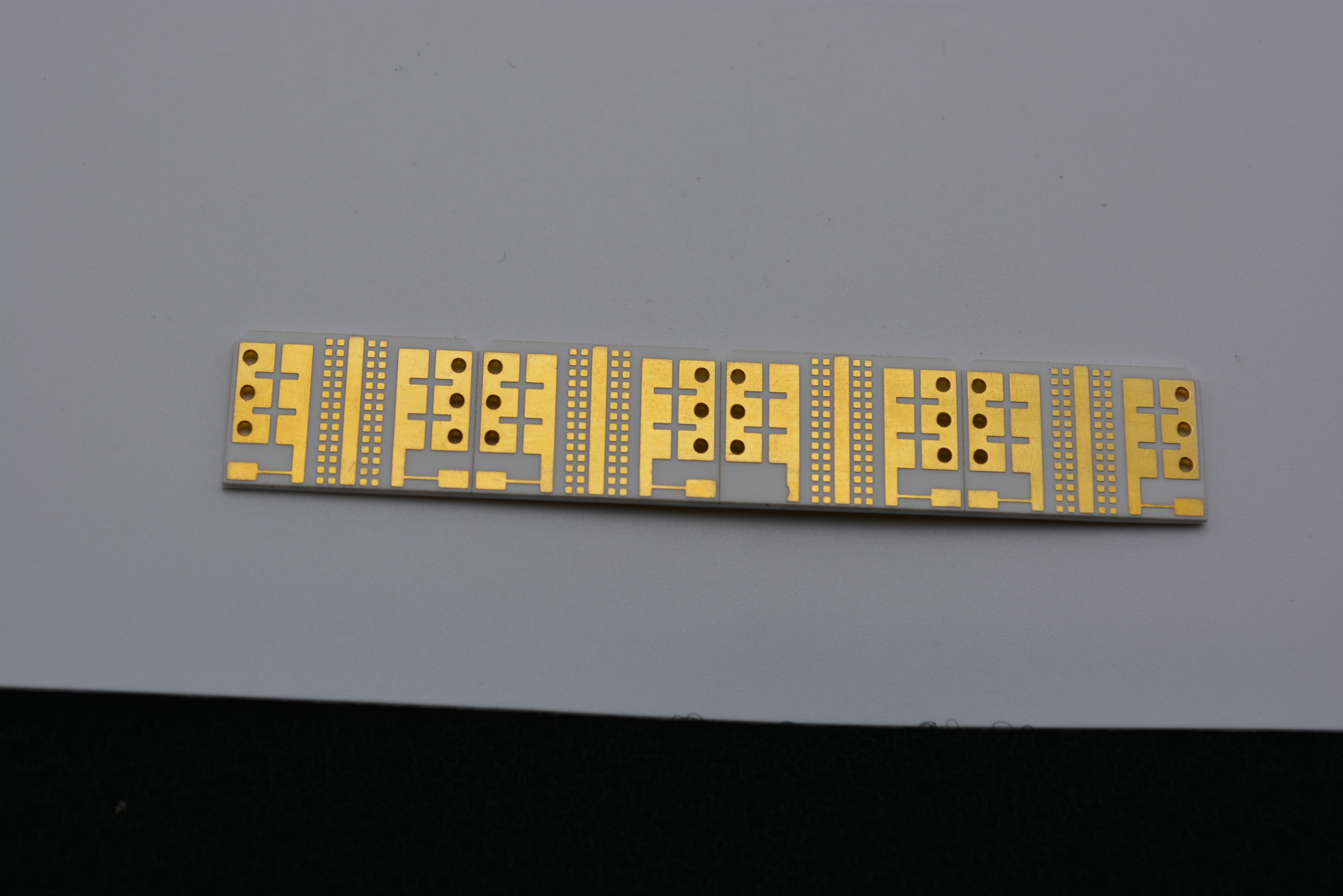
Circuit Patterning
Circuit patterning is an important part of making pcbs. You need to make exact circuit paths on each ceramic layer. LT CIRCUIT uses advanced ways to make sure your printed circuit boards are high quality. The table below shows some common ways:
Method/Process | Description | Advantages |
|---|---|---|
Thin Film Method (DPC) | Put down a metal seed layer, then use photolithography and etching to make fine lines. | Makes lines as small as 20μm; good for high-density circuits. |
Direct Copper Bonding (DBC) | Attach copper foil right to the ceramic at high heat. | Moves heat well; used in power modules. |
Use special solders to join metal to ceramic for strong, reliable joints. | Handles temperature changes very well. | |
Tape Casting + Screen Printing | Print thick film conductive pastes on ceramic sheets, then heat to set the pattern. | Saves money and works well for multilayer designs. |
You can also use laser micro-etching for tiny features or waterjet cutting for smooth edges. These ways help you make complex multilayer pcb circuits that work well.
Note: LT CIRCUIT’s good pcb manufacturing process uses these advanced patterning ways to make sure your multilayer ceramic pcbs work well in tough places.
Now you know how making multilayer ceramic pcbs starts with careful design, goes through careful layer preparation, and ends with advanced circuit patterning. Each step helps you build strong, reliable multilayer pcb solutions for today’s electronics.
Layer Stacking
Lamination
First, you get each layer ready for stacking. You put the ceramic layers and circuit patterns in order. A lamination press pushes down very hard for up to two hours. The pressure is over 33,000 lbf/ft². The heat level depends on the ceramic type, so always check the datasheet. This step sticks the layers together and gets rid of air pockets. The prepreg melts and fills spaces, making the board strong.
Problems can happen during this step. You might see things like gaps, layers coming apart, or bending. Here is a table that shows some common problems and ways to stop them:
Defect Type | Description/Effect | Prevention/Control Measures |
|---|---|---|
Voids/White Edges | Weak bonding from low resin | Ensure enough resin in prepreg |
Delamination | Layers separate, causing failure | Use vacuum lamination, pre-bake, optimize cycle |
Layer Misalignment | Layers not aligned, causing open circuits | Use positioning holes, optical alignment |
Blistering/Bubbles | Raised areas from trapped gas/moisture | Pre-bake, cleanroom, optimize lamination |
Warpage | Board bends due to thermal mismatch | Use compatible materials, symmetrical stack-up |
Tip: Keeping the right pressure, heat, and clean work area helps you stop most problems when making multilayer pcbs.
Alignment and Registration
Getting the layers lined up right is very important. You use special holes and cameras to match up each layer. Automated optical inspection checks if every layer is in the right spot. Fancy machines can keep layers lined up within 0.05 to 0.10 mm. You also use measuring machines to double-check the placement.
Good registration needs clean holes and steady materials.
Optical systems move layers to the right place as you work.
AOI and checks during the process help you find mistakes early.
You must keep the layers stacked just right so the multilayer pcb works well. Good alignment stops shorts and broken circuits, making your multilayer pcb strong and safe.
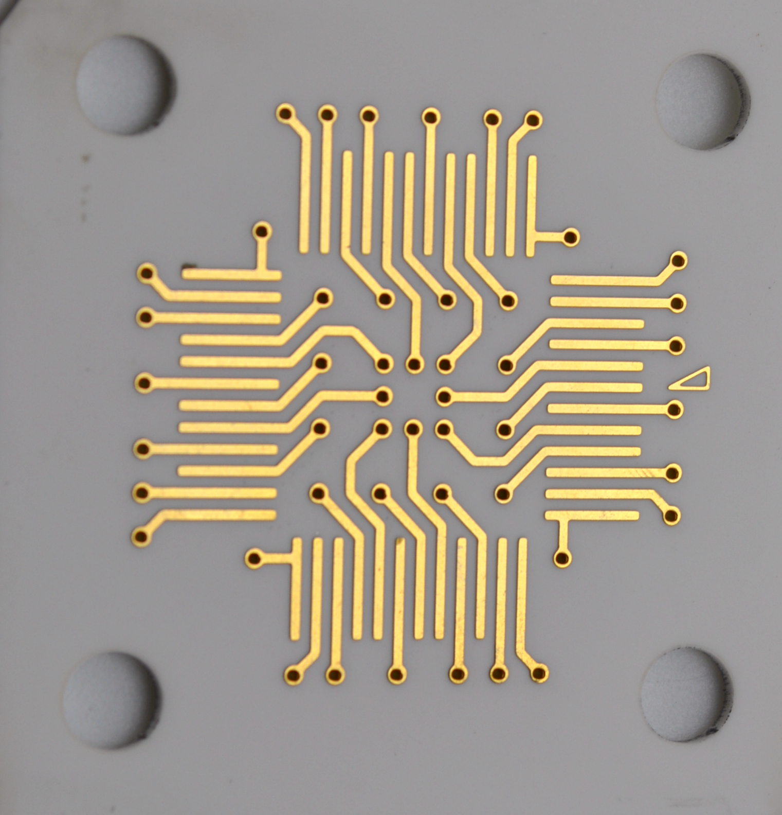
Via Formation
Drilling
To connect the layers in multilayer ceramic PCBs, you need vias. Vias are tiny holes that go through the board. You can make them with lasers or machines. Most companies now use laser drilling for small holes called microvias. Lasers like UV and CO2 can make holes as small as 50 microns. The laser cuts through the ceramic without touching it. This makes the holes clean and straight. Lasers can drill thousands of microvias every second. This step is very important for high-density multilayer boards.
Mechanical drilling was used more in the past. It can leave dust and cause cracks in the ceramic. Laser drilling gives better control and less damage. After drilling, another laser can clean the copper pads. This happens before adding metal.
Tip: The right laser settings help avoid damage. They also make sure your multilayer PCB has strong connections.
Metallization
After drilling, you fill the vias with metal. This lets electricity move between the layers. You can use silver paste, copper paste, or gold for special jobs. Filling the vias with metal makes the board strong. It also helps electricity flow well. Sometimes, you fill the whole via to make it flat. This is good if you want to put parts on top of the via.
You can pick different metallization processes for your needs. Here is a table with some common ways:
Metallization Process | Key Materials | Advantages & Suitability for Multilayer Ceramic PCB Vias | Typical Applications & Notes |
|---|---|---|---|
HTCC | Alumina + Mo/W | Very strong, seals well, good for reliable multilayer modules | Used in aerospace and military |
LTCC | Glass-ceramic + Ag/Au | Lower heat, good for RF, works for reliable multilayer circuits | Used in telecommunications and radar |
AMB | AlN + Cu + Ti braze | Strong copper bond, handles heat changes, good for high-current multilayers | Used in power electronics and industrial drives |
DPC | AlN/Al2O3 + Copper | Very exact, strong bond, good for high-density multilayer circuits | Used in LED, RF, and power circuits |
DBC | AlN/Al2O3 + Thick Copper | Thick copper, moves heat well, best for thick copper multilayer boards | Used in IGBT modules and car inverters |
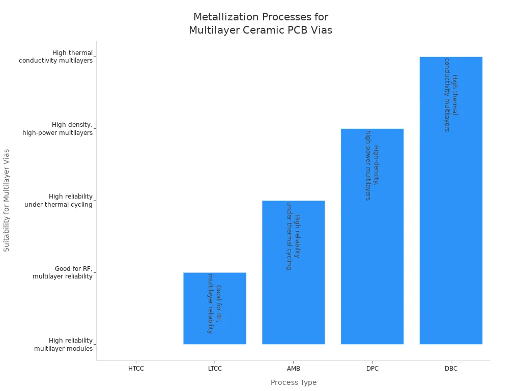
You should choose the metallization process that fits your board’s size and job. Good metallization keeps your board working well, even in hard places.
Firing and Sintering
High-Temperature Processing
Firing and sintering is a very important step. You use high heat to join the ceramic layers and metal circuits. The heat level depends on the ceramic process you pick. Here is a table that shows the usual firing temperatures for each process:
Process Type | Typical Firing Temperature | Application / Notes |
|---|---|---|
LTCC | Around 850°C | Good for high-frequency signals and RF modules. |
HTCC | Above 1600°C | Used in aerospace and high-power applications. |
You can also see the sintering temperature ranges for each process in this chart:
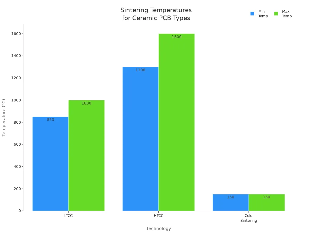
HTCC firing uses heat from 1300°C to 1600°C. This makes the ceramic particles stick together and form a solid board. LTCC firing uses lower heat, from 850°C to 1000°C. This lets you use metals like silver and copper for the circuits.
Note: Using high heat is very important. It helps make your multilayer ceramic PCB strong and dependable.
Achieving Durability
You want your multilayer ceramic PCB to last and work well. Firing and sintering make the board tough and hard. High heat makes the ceramic layers thick and strong. This helps the board resist bending, breaking, and heat damage.
HTCC makes the board the strongest. These boards can handle a lot of heat and force. That is why HTCC boards are used in planes, the military, and fast cars.
To check if your board is tough, you can use these tests:
Durability Metric | Test/Condition Description | Performance Indicator |
|---|---|---|
Adhesion Strength | Scraping test on silver traces | Minimal material loss |
Tensile and Shear Strength | Pulling and twisting tests | Strong bonding between layers |
Environmental Stability | Soaking in water, acid, and base for 500 hours | Very small change in resistance |
Thermal Aging Properties | Heating at 500°C and 800°C for up to 500 hours | Resistance stays stable at lower temperatures |
Heating Stability | Over 200 current on-off cycles between 0–350°C | High stability |
Adhesion Test | 3M Scotch tape test, 1000 times | Passes all tests |
Scratch Resistance | 1000 scratch tests | Negligible increase in resistance |
A well-fired multilayer ceramic PCB will keep working for many years. It will work even in hard places. That is why firing and sintering are so important when making these boards.
Surface Finishing
Surface Treatments
You must keep the copper pads and traces safe. Surface treatments help protect them from damage. These finishes stop the copper from rusting. They also help your board work better for a long time. Soldering is easier when you use these finishes.
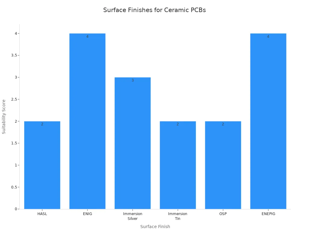
Here is a table that lists the most used surface finishes for multilayer ceramic PCBs:
Surface Finish | Why Commonly Applied to Multilayer Ceramic PCBs | Key Advantages | Limitations |
|---|---|---|---|
Hot Air Solder Leveling (HASL) | Cost-effective general-purpose finish | Good solderability, inexpensive | Not suitable for fine-pitch components, limited shelf life due to solder oxidation |
Electroless Nickel Immersion Gold (ENIG) | Preferred for high-reliability, fine-pitch, and high-frequency applications | Excellent solderability, long shelf life, corrosion resistance, good electrical conductivity | Higher cost, risk of black pad defects, complex process |
Immersion Silver | Cost-effective alternative with good solderability and conductivity | Smooth finish, good for RF and high-frequency use, suitable for fine-pitch | Tarnishes over time, limited shelf life, sensitive to environmental conditions |
Immersion Tin | Affordable finish compatible with lead-free soldering | Good solderability, suitable for fine-pitch | Limited shelf life, prone to oxidation and tin whiskers, less reliable in harsh environments |
Organic Solderability Preservatives (OSP) | Economical and environmentally friendly | Protects copper from oxidation, flat surface ideal for BGAs and fine-pitch | Limited durability, short shelf life, not suitable for multiple reflow cycles |
Electroless Nickel Electroless Palladium Immersion Gold (ENEPIG) | Premium finish for demanding applications | Exceptional solderability, corrosion resistance, long shelf life, supports gold wire bonding | Higher cost |
ENIG and ENEPIG are best for boards that need to last. They help make strong solder joints and stop rust. These finishes also keep your board safe from damage. Immersion silver and tin are good if you want a smooth board and lower price.
Picking the right surface finish helps your multilayer ceramic PCB last longer and makes putting parts on easier.
Assembly
After you finish the surface treatment, you start assembly. This step puts all the parts on your multilayer ceramic PCB. You need a clean and flat board for this step. ENIG and ENEPIG finishes help make strong solder joints. They also keep your board safe from rust, which is good for long use.
During assembly, you put each part in the right place. You can use machines or do it by hand. Soldering connects the parts to the board. Good finishes make this step easier and help stop weak joints.
You should always check your board after assembly. Look for missing parts or bad solder joints. Careful assembly gives you a multilayer ceramic PCB that works well in any device.
Quality Control
Quality control is very important when making multilayer ceramic PCBs. You want each board to be safe and work well. LT CIRCUIT checks every board with special tests and inspections. This helps the boards work in many places.
Inspection Methods
You need to find problems early in the process. Different ways of checking help you see mistakes before customers get the boards.
Inspection Method | Technique Used | Purpose |
|---|---|---|
Optical Inspection | Automated Optical Inspection | Find surface defects and misalignments |
Electrical Testing | Impedance and Continuity Tests | Check electrical connections and performance |
X-ray Inspection | X-ray Imaging | Reveal hidden defects like voids or delamination |
In-Circuit Testing | Test Probes and Fixtures | Test component function and circuit connections |
Functional Testing | Power-up and Simulation | Confirm the board works in real conditions |
People also use manual checks, flying probe testing, and Hi-Pot testing. These extra steps help find bad solder joints, missing parts, or insulation issues.
Tip: Using more than one inspection method gives the best results for quality control.
Reliability Testing
You want your multilayer ceramic PCBs to last a long time. Reliability tests show how boards handle heat, water, and stress. LT CIRCUIT uses strict rules to test every board.
Environmental tests put boards in hot and wet places for a long time.
Salt spray tests see if the boards can resist rust.
Vibration and shock tests shake and drop the boards to check strength.
Thermal shock tests move boards from hot to cold to find weak spots.
Electrical tests check if the board’s connections and insulation work.
Mechanical tests bend and peel the boards to check toughness.
These tests help you know the boards will work in hard places. LT CIRCUIT’s careful quality control means you get good boards every time.
Applications
Industry Uses
Multilayer ceramic pcb boards are used in many fields. These boards help make devices that need to work well and last long. The table below shows where each industry uses multilayer ceramic pcb technology and what they use it for:
Industry | Primary Application Areas |
|---|---|
Automotive | Advanced communication systems like 4G, 5G, WiFi, Bluetooth, GPS, and NFC |
Telecommunications | Cell phones use multilayer pcbs for processors, memory, radio circuits, touchscreen drivers, and cameras |
Industrial Controls | Used in programmable logic controllers, CNC machines, robots, and power generators |
Used in ultrasound, X-ray, ECG/EEG monitors, and defibrillators | |
Aerospace Engineering | Used in satellites, space stations, and probes for command, data, power, and instruments |
Nuclear Applications | Used in nuclear detection, security systems, and radiation sensor data transmission |
GPS Systems | Used in GPS receivers for accurate timing of high-frequency signals |
Test & Measurement | Used in oscilloscopes, spectrum analyzers, and function generators for microwave and RF signals |
Traffic Management | Used in smart transportation systems with traffic sensors, cameras, and message signs |
Consumer Electronics | Used in cell phones and small repeater pcbs for better signals |
These multilayer ceramic pcb boards are found in cars, satellites, and more. They help make devices smarter and more dependable.
Performance Advantages
Multilayer ceramic pcb boards give you many good things. These boards work well in hard places and help your devices last longer.
They move heat away fast, so your device stays cool.
The ceramic pcb keeps electricity from leaking, so signals stay clear.
Multilayer boards can handle shaking, pressure, and heat without breaking.
You can make small and tricky devices because these boards are compact.
These boards work with high frequencies and keep signals strong, which is good for RF and microwave jobs.
The copper and ceramic stick together well, so layers do not come apart.
You can use these boards in medical and space devices because they resist radiation and tough conditions.
Tip: Using multilayer ceramic pcb boards helps you build devices that work well in any field.
LT CIRCUIT Solutions
Product Range
LT CIRCUIT has many multilayer ceramic PCB choices. These products work for different electronics jobs. Some boards are for high-density needs. Others help with heat problems. The table below lists some main options you can pick:
Product Type / Feature | Layer Range | Min Line Width | Materials | Special Features / Surface Finish | Thermal Conductivity |
|---|---|---|---|---|---|
OEM Precision Ceramic Multilayer PCB | 1-8 | 0.1mm | N/A | Immersion Gold Surface | N/A |
Al2O3/ALN Electronics Ceramic PCB | N/A | 0.1mm | Al2O3/ALN | Black Solder Mask | N/A |
ITEQ IT180 High Density Multilayer PCB | 10 | N/A | ITEQ IT180 | N/A | |
14 | N/A | TG180 IT180 | High TG, Blind & Buried Holes | N/A | |
ATE Testing Multilayer PCBs | 26 | N/A | TG180 IT180 | N/A | N/A |
DFM Multilayer Ceramic PCB | N/A | N/A | N/A | Immersion Gold, ENIG Finish, Temp Resistant | N/A |
Advanced Ceramic PCB with Immersion Gold | N/A | N/A | Al2O3 | Immersion Gold Surface | 170 W/mK |
ENIG 3U" 8 Layer PCB Board | 8 | N/A | ShengYi S1000 | Impedance Controlled | N/A |
Black Ceramic PCB Board | 1-8 | N/A | Al2O3/ALN | Thermal Conductivity | 170 W/mK |
LT CIRCUIT makes boards for cars, phones, and planes. This company is a trusted ceramic pcb maker. They help with both small and big projects.
Customization Options
You have lots of ways to change your multilayer ceramic PCB at LT CIRCUIT. Here are some main choices:
DFM support helps you design a board that is easy to build.
Prototyping lets you try your design before making many boards.
You can order just a few boards or a lot, as needed.
Engineers help you fix design problems early.
You can pick finishes like ENIG or nickel-palladium gold.
Choose materials like Al2O3 or AlN for different heat needs.
Pick solder mask colors, such as black, and set line width or spacing.
Boards can work in cold or hot places, from -50°C to 150°C.
LT CIRCUIT gives help from start to finish, including fixing problems and updates.
You get advice on design and handling so your board fits your project.
LT CIRCUIT’s all-in-one service helps you get a custom board that fits your needs.
You have learned that multilayer ceramic pcbs use special steps and materials. These boards are strong and dependable. Multilayer ceramic pcbs can handle heat and do not get damaged by chemicals. They also work well in hard places. If you pick LT CIRCUIT, you get multilayer ceramic pcbs that can handle lots of power. They last a long time and work for your hardest projects.
FAQ
What makes multilayer ceramic PCBs better for high-power devices?
You get better heat management with ceramic PCBs. The ceramic material moves heat away fast. Your device stays cool and works longer.
Tip: Use ceramic PCBs for power electronics or LED lighting.
Can you use multilayer ceramic PCBs in harsh environments?
Yes, you can. Ceramic PCBs resist heat, chemicals, and vibration. Your board will keep working in tough places like factories or cars.
How do you choose the right surface finish for your PCB?
Check your device needs. ENIG works well for fine-pitch parts. HASL costs less. Immersion silver fits high-frequency jobs.
Finish | Best Use |
|---|---|
ENIG | Fine-pitch, long life |
HASL | General, low cost |
Silver | RF, high frequency |
See Also
A Comprehensive Guide To Manufacturing Multilayer Ceramic PCBs
Step-By-Step Overview Of The Multilayer PCB Manufacturing Process
Advanced Production Techniques For Heavy Copper Multilayer PCBs
Essential Skills Required For Designing Multilayer PCB Layouts
Understanding Multilayer PCBs And Their Role In Modern Electronics