Top 10 Benefits of HDI PCBs for Modern Electronics
You experience the advantages of hdi pcb every time you use a smartphone or wearable device. Today, more than 49% of modern electronics depend on HDI PCBs, compared to just 37.5% for traditional PCBs. The advantages of hdi pcb include smaller sizes, enhanced reliability, and superior performance. LT CIRCUIT is at the forefront of delivering high-quality HDI PCB solutions that showcase these benefits.
Key Takeaways
HDI PCBs enable miniaturization, allowing for smaller and lighter devices without sacrificing performance.
High component density in HDI PCBs lets you add more features to your products, making them more advanced and efficient.
Improved electrical performance and signal integrity in HDI PCBs ensure faster and clearer communication in modern electronics.
HDI PCBs Overview
Definition
You may wonder what sets HDI PCBs apart from other printed circuit boards. HDI stands for high-density interconnect. This technology allows you to fit more components and connections into a smaller space. HDI PCBs use advanced materials and special techniques, such as laser drilling, to create tiny holes called micro-vias. These micro-vias connect different layers inside the board, making the design much more compact and efficient. You often find HDI PCBs in devices that need to be small but powerful, like smartphones and medical equipment.
Key Features
You can see the main differences between HDI PCBs and conventional PCBs in the table below:
Characteristic | HDI PCBs | Conventional PCBs |
|---|---|---|
Micro-Vias | Yes, with diameters ≤ 100 microns | No |
Advanced Materials | High-grade materials like polyimide | Typically FR4 |
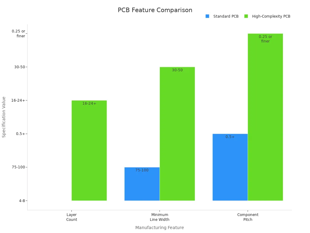
Layer Count | 8 to 20 layers or more | Usually fewer than 8 |
Interconnect Density | Higher density, pitch ≤ 50 microns | Lower density |
Fine Line Traces | Widths ≤ 50 microns | Wider traces |
Buried and Blind Vias | Commonly used for internal connections | Rarely used |
Surface Finishes | Gold or nickel plating | Various finishes |
Specialized Fabrication | Laser drilling and high precision imaging | Standard techniques |
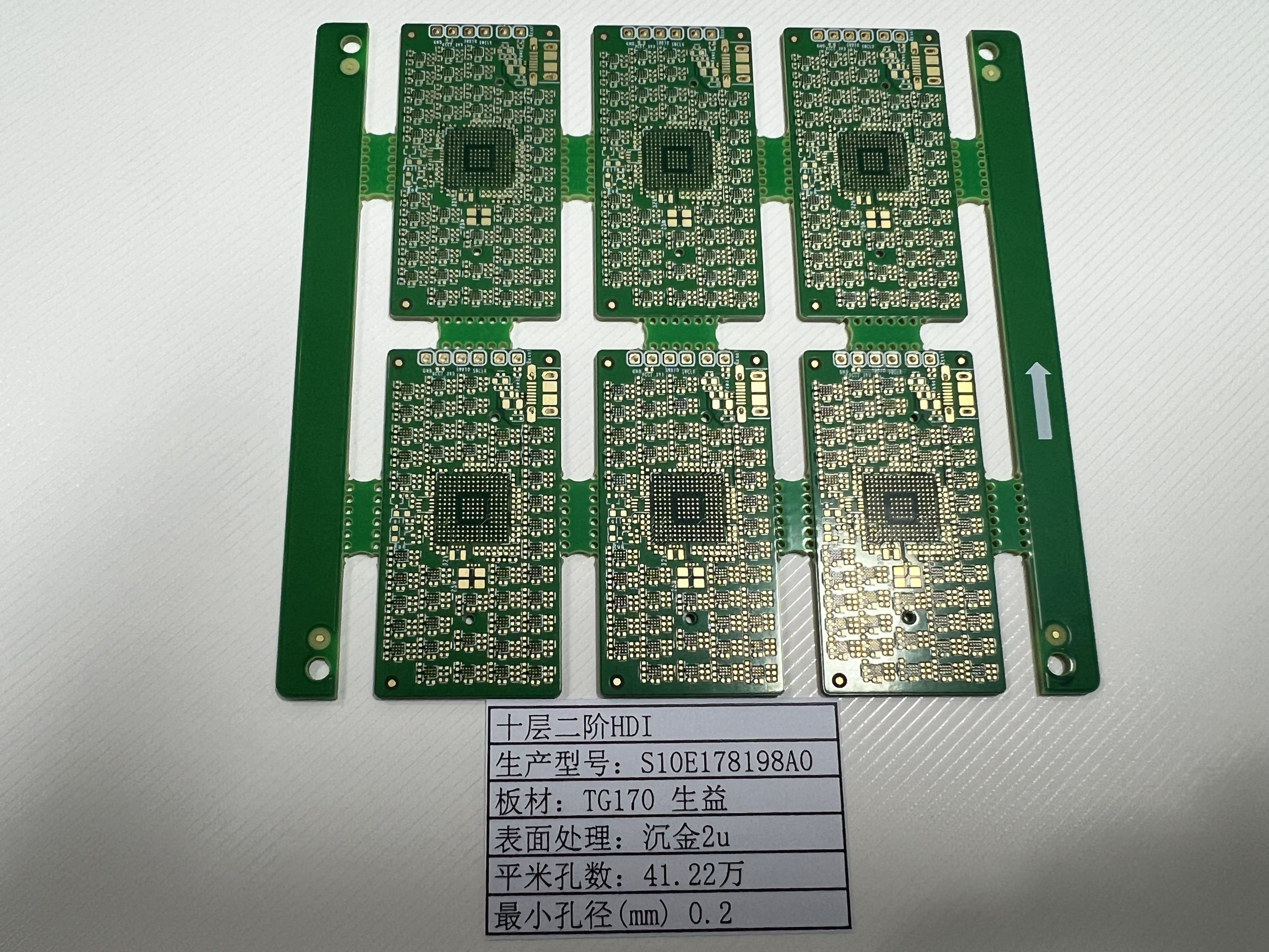
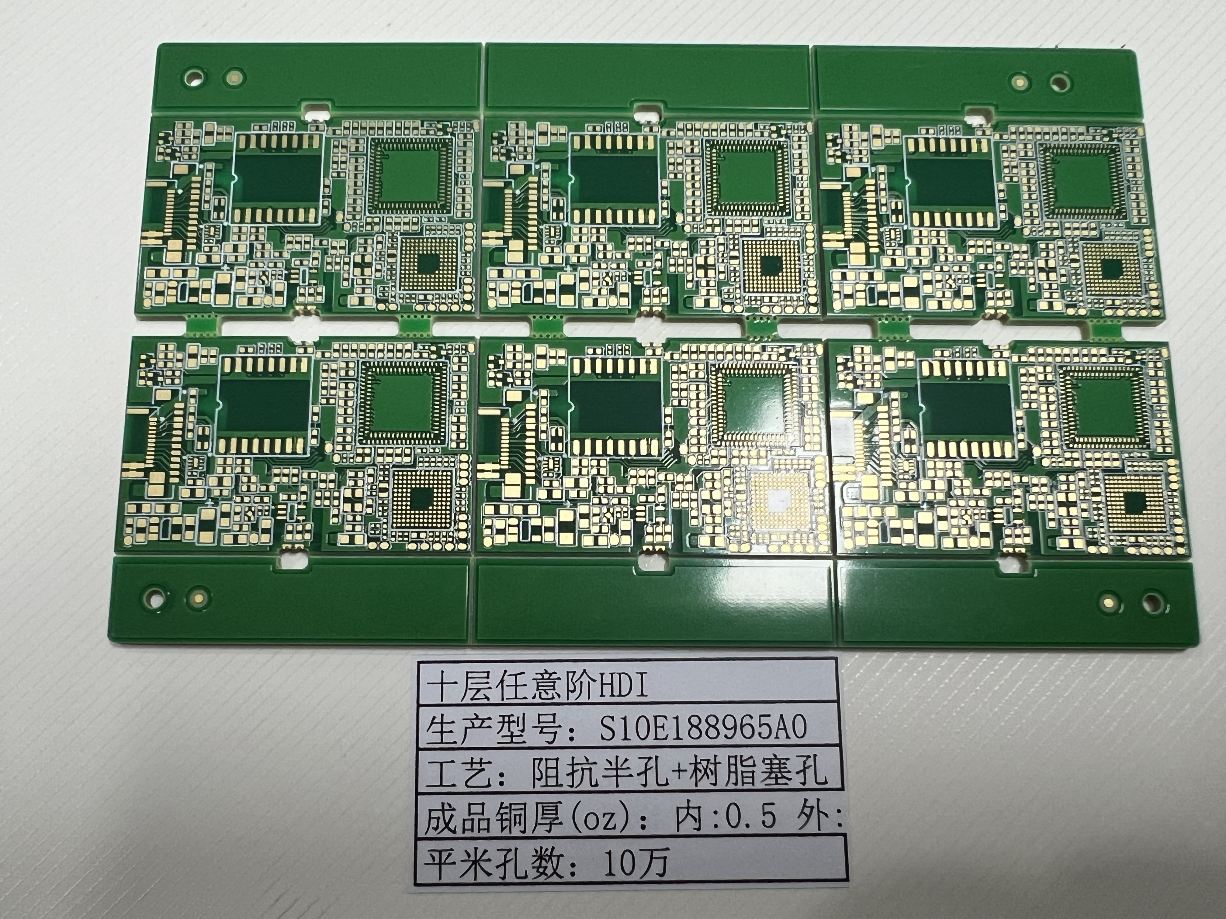
LT CIRCUIT leads the way in HDI PCB innovation. You benefit from their use of advanced materials and precise laser drilling, which boost reliability and performance. LT CIRCUIT uses strict process control and Automated Optical Inspection to ensure every micro-via meets high standards. Each board goes through thorough testing, such as Flying Probe Tests for prototypes and E-tests for larger batches. LT CIRCUIT’s expertise supports industries like aerospace, medical, and telecommunications, giving you confidence in every product.
Advantages of HDI PCBs
You see the advantages of hdi pcb every time you use a modern electronic device. These boards change the way you think about circuit design. Let’s explore how high-density interconnection technology brings real benefits to your projects.
Miniaturization
You want your devices to be smaller and lighter. HDI PCBs make this possible. The miniaturization of boards happens because you can fit more circuitry into less space. Microvias, which are tiny holes drilled with lasers, allow you to connect layers without taking up much room. This means you can design smartphones, tablets, and wearables that are thin and powerful.
LT CIRCUIT uses laser drilling to create microvias, making your devices more compact and efficient.
You notice that HDI PCBs compress more circuits into a smaller area than standard boards. This is why you find them in products like smartwatches and medical implants. You get more features without increasing the size.
High Component Density
You need to add more features to your products. HDI PCBs help you achieve high component density. With high-density interconnection, you use microvias, thin cores, and multiple layers to pack more components onto each board. This lets you design advanced devices without making them bulky.
Microvias let you place chips and resistors closer together.
Tighter trace spacing means you can route more signals in the same area.
Build-up layers allow you to stack circuits vertically.
You see these advantages of hdi pcb in laptops, cameras, and other high-tech devices. LT CIRCUIT’s advanced manufacturing ensures every layer is precise, so you get reliable performance even in complex designs.
Electrical Performance
You expect your devices to work fast and respond quickly. HDI PCBs deliver better electrical performance because they shorten the distance signals must travel. Microvias and ultra-fine traces reduce signal loss and boost speed. You benefit from high-definition data transfer, which is essential for computers and phones.
Shorter paths between components mean less signal delay.
Advanced materials with low dielectric constants help signals move faster.
Optimized routing reduces electrical noise.
LT CIRCUIT uses automated optical inspection and X-ray checks to ensure every board meets strict standards. You get the advantages of hdi pcb in every product, from gaming consoles to industrial controllers.
Signal Integrity
You want your devices to send and receive clear signals. HDI PCBs offer better signal integrity, especially in high-speed and high-frequency circuits. Microvias and optimized stackup designs help prevent signal loss and interference. High-density wiring lets you connect more circuits without causing crosstalk.
Laser-drilled microvias improve transmission rates.
Careful layer stacking boosts electromagnetic compatibility.
Compact layouts reduce the risk of signal degradation.
You rely on these advantages of hdi pcb in devices like routers and 5G base stations. LT CIRCUIT’s expertise in high-density interconnection ensures your products maintain better signal integrity, even in demanding environments.
Reliability
You need your electronics to last. HDI PCBs give you high reliability because they use quality materials and advanced processes. Microvias and sequential lamination reduce thermal stress and mechanical strain. Shorter interconnections lower the chance of signal problems.
HDI PCBs show lower failure rates under thermal cycling.
Stronger connections mean your devices can handle tough conditions.
LT CIRCUIT uses flying probe tests and custom solutions to meet your needs.
You trust these advantages of hdi pcb in mission-critical applications, such as medical devices and aerospace systems.
When you choose LT CIRCUIT, you get the full range of advantages of hdi pcbs. Their advanced manufacturing techniques, like laser drilling and automated inspection, guarantee top performance and durability for your products.
Applications of HDI PCBs
Consumer Electronics
You see the applications of hdi pcbs every day in your favorite gadgets. HDI PCBs make it possible for you to enjoy slim smartphones, powerful tablets, and advanced wearables. Manufacturers use microvias to connect multiple layers inside these devices, which helps them pack more features into smaller spaces.
Smartphones rely on HDI PCBs to combine cameras, processors, and batteries in a compact design.
Smartwatches use microvias to fit sensors and wireless modules into a tiny case.
Tablets benefit from microvias, allowing for thin profiles and efficient layouts.
Wearables depend on HDI PCBs for lightweight and comfortable designs.
LT CIRCUIT offers a wide range of HDI PCB options for these products. You can choose from different solder mask colors, surface finishes, and testing services to match your needs.
Telecommunications
You depend on fast and reliable communication. HDI PCBs play a key role in telecommunications equipment by using microvias to create precise connections. These boards improve signal integrity, which is essential for high-speed data transfer. Microvias help reduce signal loss and crosstalk, so your devices can handle large amounts of data without errors. LT CIRCUIT’s advanced manufacturing ensures every board meets strict standards for performance and reliability.
Industrial Devices
You expect industrial devices to work efficiently and last a long time. HDI PCBs support these goals by using microvias to increase line density and improve signal quality. This design reduces errors in data transmission and helps manage heat, which prevents overheating. LT CIRCUIT provides customized HDI PCBs for industrial equipment, offering solutions that boost reliability and efficiency in tough environments. The applications of hdi pcbs in this field help you achieve better performance and durability.
LT CIRCUIT Expertise
Innovation
You benefit from LT CIRCUIT’s drive for innovation every time you use advanced electronics. The company uses microvias to increase component density and improve signal integrity. Microvias allow you to design smaller devices with more features. LT CIRCUIT also integrates embedded components within the PCB, which saves space and reduces noise. You see faster signal movement because LT CIRCUIT uses low-loss dielectrics, especially in high-frequency applications like 5G. The company selects strong laminates and special resin to make boards durable in high-stress environments.
LT CIRCUIT’s focus on microvias and thermal vias helps manage heat and maintain performance. You get reliable devices that work well even in tough conditions.
Innovation | Description |
|---|---|
Advanced Materials | Strong laminates and resin for durability and performance. |
Low-loss Dielectrics | Faster signal transmission for high-frequency devices. |
Embedded Components | Resistors, capacitors, and chips placed inside the PCB to save space and reduce noise. |
Improved Thermal Management | Thermal vias and high-Tg materials to control heat. |
You notice continuous ground planes in LT CIRCUIT’s designs. These act as shields against electromagnetic interference, which is important for modern electronics.
Quality Assurance
You trust LT CIRCUIT because the company follows strict quality assurance practices. Every HDI PCB goes through multiple checks, including Automated Optical Inspection and X-ray analysis. These steps help reduce defects and ensure your board works as expected. LT CIRCUIT uses microvias in its designs, and each one is inspected for accuracy. The company meets international standards like ISO 9001, UL, and CE, so you know your product is safe and reliable.
Boards are tested with thermal cycling and impedance checks.
LT CIRCUIT follows IPC-610 Class 3 standards for high quality.
Lead-free manufacturing meets RoHS regulations for environmental safety.
Continuous improvement uses AI models and Digital Twin Technology.
Customers praise LT CIRCUIT for excellent support and clear communication. You receive high-quality products at fair prices, and you can rely on LT CIRCUIT’s expertise in microvias for critical applications in telecom, aerospace, and medical devices.
Cost and Production Efficiency
High-Volume Manufacturing
You want your products to be affordable and efficient. HDI PCBs help you achieve this in high-volume manufacturing. These boards use blind and buried vias, which allow you to fit more connections into a smaller area. Laser-drilled microvias make it possible to create very small holes, saving space and reducing the number of layers you need. This efficient layout means you can use fewer layers overall.
HDI PCBs reduce board size and weight, which lowers shipping and material costs.
You benefit from enhanced electrical performance, especially in high-speed devices.
When you produce HDI PCBs in large batches, the per-unit cost drops.
Fewer layers and smaller boards mean you save money on every unit.
You see these advantages in industries that require thousands of units, such as consumer electronics and telecommunications. Smaller, lighter boards also make your products easier to handle and assemble.
Customization
You may need unique features for your project. LT CIRCUIT offers custom solutions to match your requirements. You can choose from different surface finishes, such as ENIG, HASL, or immersion silver. If you want a specific look, you can select from a variety of solder mask colors. LT CIRCUIT also supports embedded components, which help you design even smaller devices.
LT CIRCUIT uses high-precision flying probe testers to check each board.
Intelligent AOI optical inspection instruments catch any defects early.
Optical microscopes, impedance testers, and hole copper testers ensure thorough inspection.
Testing services like flying probe tests and E-tests verify performance before delivery.
You receive boards that meet your exact needs and pass strict quality checks. This level of customization and testing gives you confidence in every order.
Design Flexibility
Layer Stacking
You gain more freedom in your designs with HDI PCBs because of their advanced layer stacking. This process lets you build boards with many layers, each serving a unique function. You can use fewer layers to achieve the same results as traditional PCBs, which makes your devices lighter and easier to assemble. Layer stacking also improves the strength and reliability of your boards.
Evidence Description | Contribution to Design Capabilities |
|---|---|
Layer aggregation and lamination process enhances strength and reliability of PCBs. | Ensures durability and performance in compact electronic devices. |
Stackup design enhances density and reduces interlayer crosstalk. | Allows for more efficient use of space and improved signal integrity. |
Accommodates more connections with lower layer count than traditional PCBs. | Enables the design of more compact and powerful electronic devices. |
Sequential lamination process for stackup fabrication. | Provides precise control over layer arrangement, enhancing overall PCB performance and design flexibility. |
You can see the advantages of hdi pcb when you use blind and buried vias. These features give you more layout options and help you fit more connections into a smaller space. LT CIRCUIT uses sequential lamination to ensure each layer is placed with precision, giving your products better performance and reliability.
Advanced Technologies
You can design products that use the latest technologies with HDI PCBs. These boards support miniaturization, which helps you create smaller and more efficient devices. You can use HDI PCBs in 5G, IoT, and wearable devices, where space and performance matter most.
HDI PCBs let you place components on both sides of the board.
You can use microvia technology to increase routing density and reduce signal interference.
Fine line traces allow you to route complex circuits without losing performance.
LT CIRCUIT gives you the tools to take full advantage of these features. You can design high-pin-count BGAs with pitches as low as 0.4 mm. You also benefit from advanced routing techniques, such as via-in-pad and stacked microvias. These options make your designs more flexible and powerful, showing the true advantages of hdi pcb in modern electronics.
Addressing Common Concerns
Cost Considerations
You may worry about the cost of HDI PCBs when planning your next project. Several factors can affect the price:
Materials: High-quality copper and advanced substrates increase costs.
Design Complexity: More layers and microvias require extra steps and resources.
Production Volume: Large orders lower the cost per unit because of economies of scale.
Board Size and Shape: Bigger or unusual shapes need more materials and special handling.
Layer Count: Boards with many layers take longer to produce.
Surface Finish: Choices like gold or silver finishes change the final price.
You can manage costs by working with LT CIRCUIT. The team helps you select materials and finishes that fit your budget. You get advice on design choices that balance performance and price. LT CIRCUIT offers competitive pricing for high-volume orders, making advanced HDI PCBs more affordable.
Manufacturing Complexity
You might think HDI PCBs are too complex to produce. LT CIRCUIT uses advanced technology to handle these challenges. The company builds boards with up to 24 layers and microvias as small as 30μm. You benefit from precise manufacturing and strict quality checks.
Capability | Industry Average | LT CIRCUIT Offering |
|---|---|---|
HDI Micro-via Size | 50μm - 75μm | As small as 30μm |
Rigid-Flex Bend Cycles | 10,000 - 50,000 cycles | Over 100,000 cycles |
3D Assembly Density | Limited stacking | Dense vertical stacking |
You face challenges like routing congestion and thermal management. LT CIRCUIT uses design tools and thermal simulation software to solve these problems. The team works with you from the start to make sure your design matches their manufacturing strengths. You get reliable boards, even for the most demanding applications.
You see HDI PCBs powering the future of electronics. LT CIRCUIT stands out for reliability and innovation:
Used in automotive, medical, aerospace, and consumer electronics
Advanced materials and multilayer designs
Meets strict performance and reliability standards
The HDI PCB market will grow rapidly as new technologies emerge. Visit LT CIRCUIT’s website to explore solutions.
FAQ
What makes HDI PCBs different from standard PCBs?
You get more connections in less space with HDI PCBs. Microvias and fine lines allow you to design smaller, faster, and more reliable devices.
Can you use HDI PCBs for high-frequency applications?
Yes!
You achieve better signal integrity with HDI PCBs.
These boards work well in 5G, Wi-Fi, and advanced communication devices.
How does LT CIRCUIT ensure HDI PCB quality?
Step | Benefit |
|---|---|
Automated Inspection | Catches tiny defects |
Flying Probe Test | Confirms board function |
X-ray Analysis | Checks inner layers |
You receive boards that meet strict quality standards.
See Also
Explore Cutting-Edge Techniques for HDI PCB Prototyping
Advantages of LDI Machines in HDI PCB Circuit Production
Evaluating Cost-Effectiveness of Advanced HDI PCB Technologies
Saving Project Costs with Quick Turn HDI PCBs in 2025
Compact, Durable, Intelligent: The Future of HDI Rigid Flex PCBs