Key Advantages and Performance Features of Ultra HDI PCBs
Ultra hdi pcb technology offers unique advantages over standard options. Electronics professionals are witnessing rapid adoption of ultra hdi pcb due to several factors:
The market for ultra hdi pcb grows as demand for miniaturization and high-speed data increases.
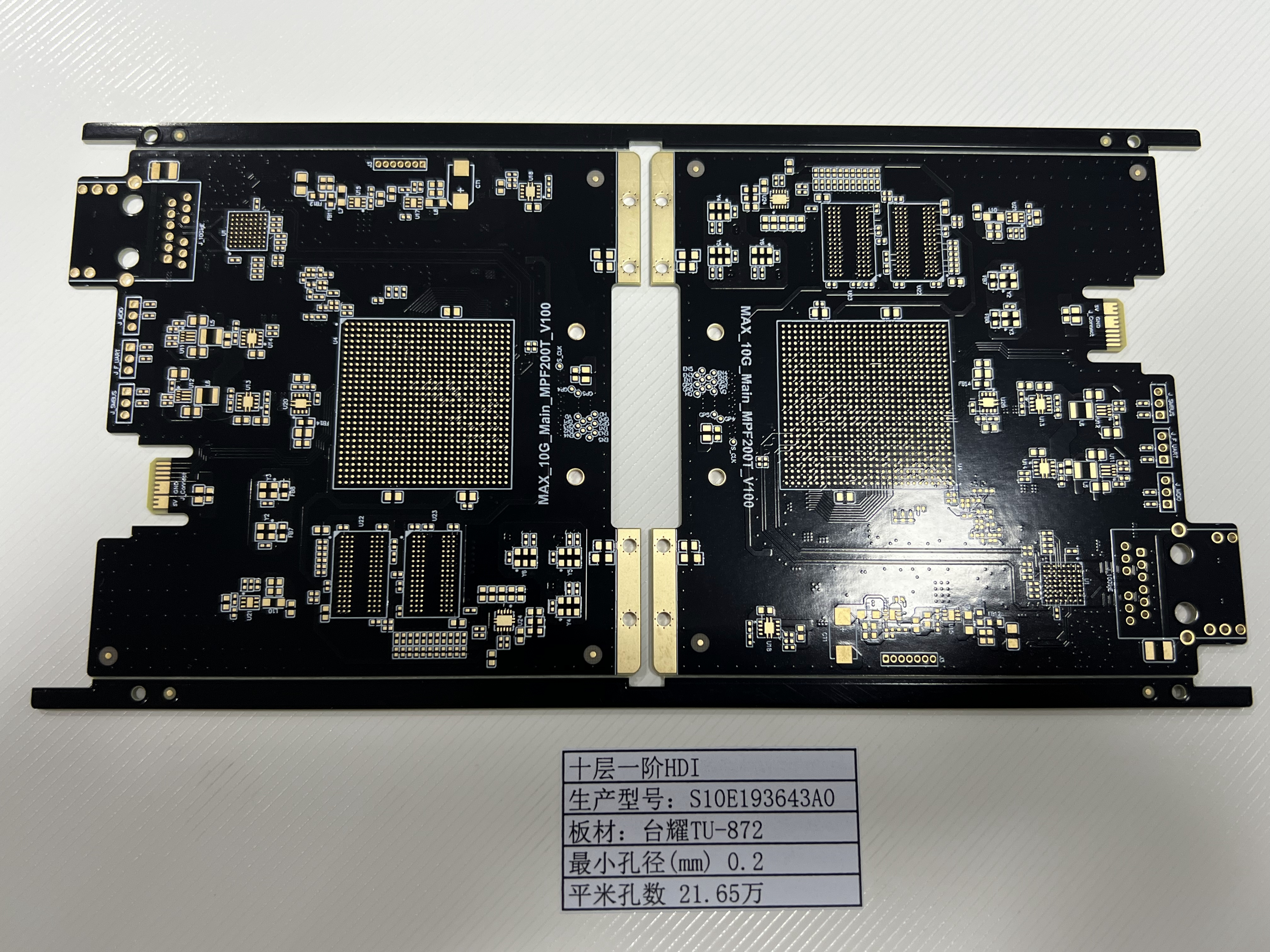
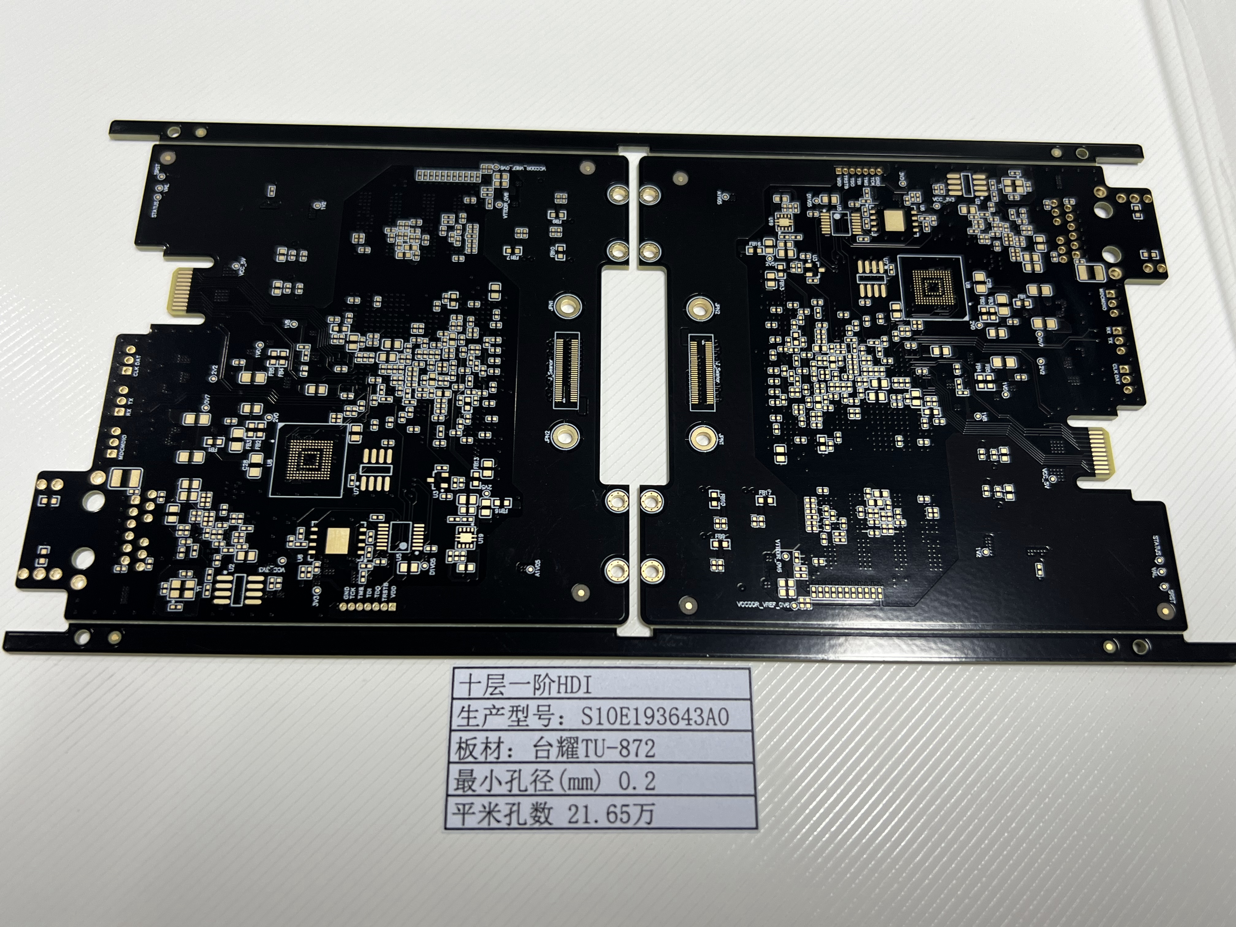
Ultra hdi pcb enables higher component density and design optimization. LT CIRCUIT leads in ultra hdi pcb manufacturing and innovation.
Key Takeaways
Ultra HDI PCBs enable higher component density, allowing for more functions in smaller devices, which is essential for modern electronics.
These boards improve signal integrity by reducing crosstalk and signal loss, leading to better performance in high-speed applications.
Advanced thermal management features in Ultra HDI PCBs help dissipate heat effectively, ensuring reliable operation in compact and high-performance devices.
Ultra HDI PCB Overview
What Is Ultra-HDI?
Ultra-hdi describes a new generation of pcb design that pushes the boundaries of miniaturization and performance. Engineers use ultra-hdi pcbs to achieve higher component density and advanced capabilities in modern electronics. These boards feature extremely fine conductor widths and spacing, often reaching 50 microns or less. The microvias in ultra-hdi pcbs measure under 75 microns in diameter, allowing for more connections in a smaller area. Ultra hdi pcb technology supports thinner dielectric layers, which improves signal transmission and overall performance.
Ultra-hdi pcbs enable designers to create compact devices with powerful functions. This technology supports applications that demand high-speed data and reliable operation.
Key Features
Key features of uhdi pcbs set them apart from standard hdi boards. The table below highlights important technical specifications:
Parameter | Features |
|---|---|
Conductor width/spacing | |
Dielectric thickness | <50 µm (2 mil) |
Microvia diameter | <75 µm (3 mil) |
Ultra-hdi pcbs use high-performance laminates with low dielectric constant and dissipation factor. These materials help maintain signal integrity and boost performance. Common pcb design methods include laser drilling for microvias and sequential lamination for buried via holes. Engineers also use sophisticated imaging to transfer circuit patterns with precision.
Available in rigid, flex, and rigid-flex board types
Hybrid constructions with ultra fine line features on select layers
Ultra-hdi offers advanced capabilities for complex pcb design. These features support demanding applications in consumer electronics, medical devices, and aerospace. Ultra hdi technology continues to drive innovation in the electronics industry.
Miniaturization Benefits

High Component Density
Ultra-hdi technology transforms the way engineers design modern pcbs. By using micro-holes and advanced manufacturing, ultra-hdi pcbs achieve much higher component density than traditional boards. Micro-holes, which measure less than 150 micrometers in diameter, allow for more electrical connections between layers. This innovation lets designers place more components in a smaller area, which is essential for devices that require a smaller form factor.
Evidence | Description |
|---|---|
Improves equipment performance by utilizing smaller parts and semiconductor packages, enhancing circuit board functionality. |
Engineers use these miniature vias to reduce pcb size and increase circuit density. The ability to fit more components on each board leads to several important benefits:
Faster signal transmission due to shorter trace lengths.
Reduced latency, which improves device responsiveness.
Lower risk of crosstalk and noise interference, thanks to optimized routing.
Support for complex circuitry, enabling advanced features in compact devices.
The miniaturization capabilities of ultra-hdi pcbs support industries that demand high performance in limited space. For example, telecommunications, healthcare, automotive, and consumer electronics all benefit from this technology. Medical implants and AI-driven systems rely on high component density to deliver powerful functions without increasing device size.
Compact Device Design
Ultra-hdi pcbs enable manufacturers to create compact and efficient interconnect solutions. These boards allow for significant reductions in thickness, weight, and area compared to standard pcbs. The table below shows measurable improvements in device size when using advanced hdi technology:
PCB Type | Weight Reduction | Area Reduction | Component Density | |
|---|---|---|---|---|
Advanced HDI PCB | Reduced to 0.4mm | Exceeds 30% | 20% (e.g., Apple Watch S6) | 20+ components/cm² |
Standard PCB | ≥1.0mm | N/A | N/A | ≤5 components/cm² |
Ultra hdi pcb designs help engineers meet the growing demand for smaller, lighter, and more powerful devices. The increased component density allows for more features and better performance in a compact package. This approach supports the development of next-generation products, such as smartwatches and autonomous vehicles, where space and weight matter.
Ultra-hdi boards also provide flexibility for designers. They can create intricate layouts and integrate multiple functions without sacrificing reliability. As a result, ultra-hdi technology continues to drive innovation in electronics, making it possible to deliver advanced capabilities in a smaller form factor.
Note: Ultra-hdi pcbs have become essential for industries that require miniaturized, high-performance electronics. Their unique design features support the ongoing trend toward smaller, smarter devices.
Signal Integrity in Ultra-HDI PCBs
Reduced Crosstalk
Ultra-hdi technology brings a new level of signal integrity to advanced pcb design. Engineers often face challenges with crosstalk, which occurs when signals from one trace interfere with another. Ultra-hdi pcbs address this issue by shortening critical signal paths and reducing parasitic capacitance and inductance. These features help lower attenuation and crosstalk, resulting in cleaner signal transmission.
A recent case study showed a 40% reduction in crosstalk between 5G and Wi-Fi signals during pre-production VNA testing. This improvement demonstrates how ultra-hdi pcbs support high-speed data transfer and maintain reliable performance in complex electronic systems.
Shorter signal paths
Lower parasitic effects
Cleaner signal transmission
These features allow designers to create pcbs for high-speed applications without sacrificing signal integrity. Devices that rely on faster transmission rates, such as smartphones and network equipment, benefit from these advancements. Improved signal integrity leads to better device performance and fewer errors during operation.
Note: Ultra hdi pcb technology helps engineers achieve robust signal integrity, even in dense and complex layouts.
High-Frequency Performance
Ultra-hdi pcbs excel in high-frequency environments. The choice of materials plays a key role in maintaining signal integrity at high speeds. Manufacturers use advanced laminates with low dielectric constant and low dissipation factor to support high-frequency applications. These materials help reduce signal loss and ensure stable performance.
Material | Dielectric Constant (Dk) | Dissipation Factor (Df) | Application Area |
|---|---|---|---|
Nelco 4000-13EP | Low | Low | High-frequency applications |
Isola I-Speed | Low | Low | High-frequency applications |
Rogers 3000 Series | Significantly improved | Low | Very high-speed circuits |
Taconic RF35 | Improved | Low | RF applications |
Arlon Cuclad | Improved | Low | High-frequency applications |
Ultra-hdi pcbs support frequency ranges above 500 MHz. Many designs operate in the GHz range, and some advanced applications reach up to 100 GHz or higher. These features make ultra-hdi the preferred choice for high-speed data transfer and demanding electronic systems.
Engineers select ultra-hdi for pcb design when they need improved signal integrity and reliable performance at high frequencies. The combination of advanced materials and precise manufacturing ensures that these pcbs deliver consistent results in high-speed environments. As a result, ultra-hdi pcbs continue to drive innovation in industries that require top-tier signal integrity at high speeds.
Thermal Management
Blind Via Technology
Blind via technology stands out as a key feature in ultra-hdi pcbs. Engineers use blind vias to connect outer layers to inner layers without passing through the entire board. This approach supports high-density routing and microvia design, which are essential for advanced electronic devices. Blind vias help manage heat by allowing thermal vias to transfer heat from hot components to inner copper planes or heat sinks. These features lower junction temperatures by 10-25°C, which improves reliability and performance.
Designers often combine blind vias with a higher layer count to spread heat more evenly. This method prevents hotspots and supports stable operation in compact devices. Blind via technology also allows for more efficient use of board space, which is important for miniaturized products.
Blind vias, when used with thermal vias, create a direct path for heat to escape from critical areas. This feature helps maintain safe operating temperatures in high-power applications.
Heat Dissipation
Effective heat dissipation is a major advantage of ultra-hdi pcbs. Engineers use several features to manage thermal performance:
Thermal vias move heat from surface components to inner layers or heat sinks.
High-thermal-conductivity materials, such as metal-core or ceramic-based laminates, offer better heat transfer than standard FR-4.
Heat sinks and thermal pads reduce operating temperatures by 10-15°C.
Multilayer designs with dedicated copper planes spread heat and lower peak temperatures by 5-10°C.
Embedded heat pipes provide exceptional heat dissipation for demanding applications.
The table below compares key parameters of traditional, HDI, and advanced HDI pcbs:
Parameter | Traditional PCB | HDI Technology | Advanced HDI |
|---|---|---|---|
Minimum via diameter | 150-200 μm | 75-100 μm | 50-75 μm |
Line width/spacing | 100/100 μm | 50/50 μm | 25/25 μm |
Component density increase | - | 200-300% | 400-500% |
Thermal resistance | 40-60°C/W | N/A | N/A |
Ultra-hdi pcbs use these features to keep devices cool, even as component density increases. This approach ensures reliable operation and extends product life.
Reliability and Durability
Robust Performance
Ultra-hdi pcbs deliver strong performance in demanding environments. Engineers use several testing methods to measure reliability. These tests help ensure that the boards can handle stress, temperature changes, and long-term use. The table below shows common reliability tests for ultra-hdi pcbs:
Testing Method | Description |
|---|---|
Qualification Coupons | Tools for parametric analysis and characterization as part of quality assessment. |
Accelerated Thermal Cycling (ATC) | A method used to evaluate the thermal reliability of PCBs under accelerated conditions. |
Highly Accelerated Thermal Shock (HATS) | Tests the PCB's ability to withstand rapid temperature changes. |
Interconnect Stress Test (IST) | Evaluates the reliability of interconnects under stress conditions. |
Thermal Cycling Testing | Involves cycling the temperature to assess the durability of the PCB connections. |
Long-term durability studies focus on microvia reliability and copper layer adhesion. These studies use accelerated life testing and cross-sectional analysis to check for issues like shoulder cracking or base copper separation. Engineers also run temperature cycling tests from -40℃ to +115℃ to simulate harsh conditions. These steps help maintain signal integrity and ensure improved reliability over time.
Lower Failure Rates
Ultra-hdi pcbs achieve lower failure rates compared to traditional boards. Several design choices and features contribute to this advantage:
Higher density and performance support next-generation electronics.
Miniaturization, high-frequency operation, and thermal management lead to improved reliability and fewer failures.
Skip-layer routing enhances signal integrity in high-bandwidth applications.
This routing minimizes losses and maintains impedance, which helps prevent signal problems.
Engineers use advanced materials and precise manufacturing to reduce common failure modes. They monitor for sleeve cracking and copper separation during testing. These efforts keep signal integrity high and lower the risk of device malfunction. As a result, ultra-hdi technology supports devices that require consistent performance and long service life.
LT CIRCUIT and Ultra-HDI Solutions
Advanced Manufacturing
LT CIRCUIT stands out in the field of ultra-hdi pcb manufacturing. The company has earned recognition for its innovative approaches and reliability. Major brands across different sectors trust LT CIRCUIT for their advanced pcbs. The company follows strict international standards, including ISO 9001, UL, and CE certifications. These achievements show a strong commitment to quality and safety.
Certification | Description |
|---|---|
UL | Underwriters Laboratories certification for safety |
CE | Compliance with EU regulations |
ISO-9001 | International quality management standard |
SGS lead-free | Certification for lead-free manufacturing |
LT CIRCUIT uses advanced capabilities to ensure high-quality results. High-speed laser drilling creates precise microvias. Vertical continuous plating provides uniform copper layers. Online AOI inspection and high-speed flying probe testing help reduce defects and improve yield rates. The company completes every step of the process in-house, which ensures accuracy and stability for all pcbs.
LT CIRCUIT’s advanced manufacturing capabilities support the most demanding ultra-hdi applications.
Customization Options
LT CIRCUIT offers a wide range of customization options for ultra-hdi pcbs. Customers can select from different materials, such as Megtron 6 and Panasonic R5775. The company supports hole sizes as small as 0.1mm and line widths down to 3mil. Board thickness ranges from 0.2mm to 6.0mm, and copper thickness can reach up to 6oz.
Customization Aspect | Options Available |
|---|---|
Material Selection | Megtron 6, Panasonic R5775 |
Hole Sizes | As small as 0.1mm |
Line and Space Widths | Down to 3mil/3mil |
Copper Thickness | 0.5oz to 6oz |
Board Thickness | 0.2mm to 6.0mm |
Solder Mask Colors | Various options |
Customers can also request special features, such as half holes or 0.25mm BGAs. LT CIRCUIT’s flexible approach allows engineers to design pcbs that meet unique project needs. These options make LT CIRCUIT a preferred partner for high-speed and complex electronic products.
Applications of Ultra-HDI PCBs
Consumer Electronics
Ultra-hdi technology drives innovation in consumer electronics. Engineers use these pcbs to create thinner smartphones, tablets, and wearable devices. Smaller features and increased routing density allow for compact designs. Every millimeter of board space matters in mobile devices. Ultra-hdi capabilities help manufacturers deliver sleeker products with advanced functions.
Application Area | Performance Improvements |
|---|---|
High-frequency, low-loss PCBs with superior signal integrity for high-speed data transmission. | |
Artificial Intelligence and HPC | Ultra-fast processing speeds and high-density interconnects for AI processors and GPUs. |
Automotive Electronics and Autonomous Vehicles | Essential for radar, LiDAR, and ADAS applications in EVs and autonomous systems. |
Flexible and Rigid-Flex PCBs | Expanding applications in medical devices and next-gen wearables due to compact designs. |
Quantum Computing and Advanced Sensors | High-density interconnects for ultra-low-latency PCB structures in future technologies. |
Designers rely on ultra-hdi capabilities to improve signal integrity and support high-speed data. These pcbs enable new features in smartwatches and wireless earbuds.
Ultra-hdi pcbs make it possible to fit more functions into smaller devices, meeting the demands of modern consumers.
Medical Devices
Medical devices require reliability and miniaturization. Ultra-hdi pcbs support complex functions in compact spaces. Engineers use multilayer structures and fine-line technology to achieve high-density connections. These capabilities are vital for implantable devices such as pacemakers and insulin pumps.
Evidence Description | Key Points |
|---|---|
Supports complex functionalities in compact spaces, enhancing reliability. | |
Fine-Line Technology | Enables high-density connections, crucial for miniaturization. |
Stability | Ensures long-term operation in medical environments, vital for devices like pacemakers and insulin pumps. |
High-density interconnects and Via-in-Pad technology reduce the size of medical pcbs. This miniaturization allows for more functions in a limited area. Medical devices benefit from improved signal integrity and stable operation.
Implantable devices need extreme reliability and biocompatibility.
Integration of power management and signal processing ensures safe operation.
Automotive & Aerospace
Ultra-hdi pcbs play a key role in automotive and aerospace electronics. These industries demand high reliability and efficiency. Engineers use ultra-hdi capabilities to enhance ADAS, EV power electronics, and infotainment systems. In aerospace, ultra-hdi supports mission-critical applications such as radar and avionics.
Application Area | Role of Ultra-HDI PCBs | Standards Met |
|---|---|---|
Automotive Electronics | Enhances reliability and efficiency in ADAS, EV power electronics, and infotainment systems. | Exceeds IPC 2226 level C standard. |
Aerospace and Defense | Improves performance and reliability in mission-critical applications like radar systems and avionics. | Conductor/trace width below 50 µm. |
Dielectric thickness below 50 µm. | ||
Microvia diameter below 75 µm. |
Ultra-hdi pcbs meet strict standards for conductor width, dielectric thickness, and microvia diameter. These features ensure signal integrity and durability in harsh environments.
Automotive and aerospace systems depend on ultra-hdi capabilities for safe and reliable operation.
Design Considerations
Layout Challenges
Engineers face unique layout challenges when working with ultra-hdi technology. The small size of features in pcb design makes thermal management and signal integrity more difficult. Designers must carefully plan the placement of components and traces. They often use simulation tools to keep impedance consistent and avoid signal loss. Collaboration with manufacturing partners helps address fabrication limits and ensures the design can be built as planned.
The table below shows common challenges and how engineers solve them:
Challenge | Solution |
|---|---|
Thermal Management | Incorporate thermal vias and heat sinks to dissipate heat effectively. |
Signal Integrity | Maintain consistent trace widths and use simulation tools for impedance. |
Manufacturing Constraints | Collaborate with PCB fabrication partners to understand their capabilities. |
Cost vs. Performance | Balance design complexity with budget constraints, prioritizing critical areas. |
Engineers must balance performance and cost in every pcb design. They focus on critical areas to get the best results from ultra-hdi pcbs.
Cost Factors
Cost plays a big role in the adoption of advanced pcb design. Several factors increase the price of ultra-hdi pcbs. The main material, CCL, makes up about 30% of the total cost. High-performance CCL materials cost more because they require extra research and careful production. When engineers design pcbs with 20 or more layers, the process becomes more complex and needs special equipment. This complexity can lower the initial yield, which raises costs.
Cost Factor | Description |
|---|---|
Rising Raw Material Costs | CCL, the core material in PCBs, accounts for ~30% of total PCB costs. High-performance CCL materials involve higher R&D and production costs, and tight supply has driven up prices. |
Increased Manufacturing Complexity | Producing 20+ layer PCBs requires greater precision and advanced processes, leading to higher costs due to the need for sophisticated equipment and control. Initial yields for AI server PCBs often fall below 50%, inflating costs. |
The cost of ultra-hdi pcb manufacturing is higher than standard HDI production because of the advanced processes.
Standard pcb unit costs range from $110-160 per square meter, while HDI pcbs cost 30-50% more.
Over time, savings from fewer layers and better performance can help offset the higher initial costs.
Careful planning in pcb design helps manage costs while still meeting the needs of modern devices.
Advantage/Feature | Description |
|---|---|
Supports compact, functional devices. | |
Reduced Signal Loss | Improves signal integrity. |
Enhanced Thermal Management | Enables efficient heat dissipation. |
Improved Reliability | Ensures mission-critical performance. |
Allows smaller, lighter products. |
LT CIRCUIT’s ultra-hdi pcbs support rapid prototyping, advanced customization, and low defect rates. Customers benefit from expert engineering and advanced pcb manufacturing. Ultra hdi pcb technology will drive future miniaturization and flexible designs in electronics.
FAQ
What makes Ultra HDI PCBs different from standard HDI PCBs?
Ultra HDI PCBs use finer lines, smaller vias, and advanced materials. These features allow higher component density and better performance in compact devices.
Can Ultra HDI PCBs handle high-frequency signals?
Yes. Ultra HDI PCBs use low-loss materials and precise manufacturing. These features support stable operation at high frequencies, making them ideal for advanced electronics.
Does LT CIRCUIT offer custom solutions for Ultra HDI PCBs?
LT CIRCUIT provides a wide range of customization options.
Customers can choose materials, thickness, copper weight, and special features to meet unique project needs.
See Also
Essential Design Factors for Reliable HDI PCB Manufacturing
Explore Innovative Techniques for HDI PCB Prototyping Now
Understanding the Design and Production of Any Layer HDI PCBs
Compact, Durable, Intelligent: The Advantages of HDI Rigid Flex PCBs
Advantages of LDI Exposure Machines in HDI PCB Circuit Production