How to Design and Manufacture Ultra-long-sized Multi-layer Circuit Boards for Advanced Applications
You want a reliable guide to take your ultra-long-sized multi-layer circuit board from concept to production. In recent years, the market for multilayer PCBs has grown rapidly, with values reaching up to USD 77.3 billion in 2023 and projections as high as USD 120.95 billion by 2032.
Precision and advanced technology matter most when you design for high-performance sectors, such as aerospace, automotive, and medical devices.
Industry | Application Type | Description |
|---|---|---|
Aerospace | Used for power, signal routing, and stability in spacecraft and satellites. | |
Medical Devices | Ultra Long Flex/Rigid | Supports wearables and imaging equipment like MRI and CT scanners. |
Automotive | Ultra Long Flex/Rigid | Routes signals in ADAS, displays, and engine control units. |
Consumer Electronics | Ultra Long Flex/Rigid | Enables flexible displays and stable device components. |
Start with careful stack-up planning, select the best materials, and keep manufacturability in mind to achieve success.
Key Takeaways
Understand application requirements before starting your project. Each industry has unique needs for ultra-long-sized multi-layer circuit boards.
Select materials carefully to match your application. Consider factors like thermal expansion, dielectric loss, and moisture absorption to ensure durability.
Follow Design for Manufacturability (DFM) principles. This helps ensure efficient production and reliable performance of your circuit boards.
Implement thorough testing and inspection methods. Use techniques like Automated Optical Inspection and X-ray to detect defects and ensure quality.
Collaborate with experts like LT CIRCUIT early in your project. Their guidance can help you navigate complex design and manufacturing challenges.
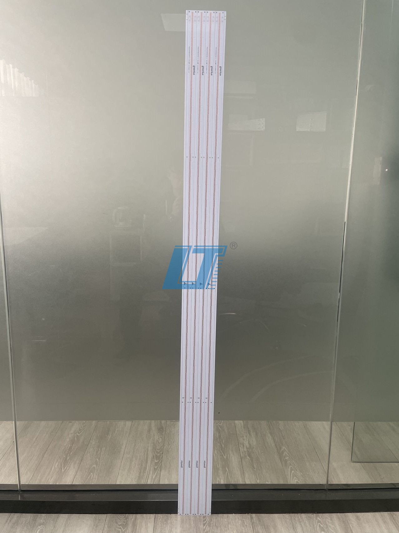
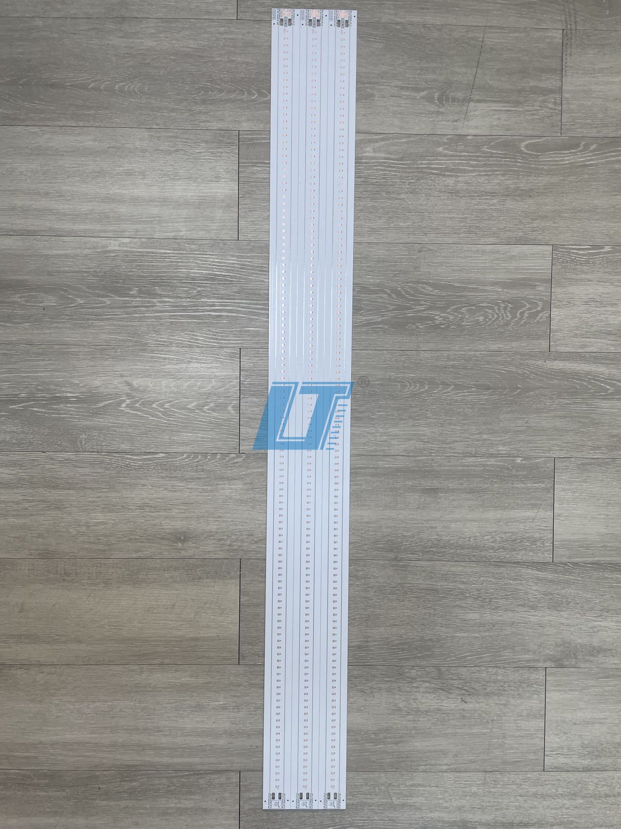
Ultra-long-sized Multi-layer Circuit Board Design
Application Requirements
When you start a project with an ultra-long-sized multi-layer circuit board, you must first understand the specific needs of your application. Each industry sets unique requirements for these advanced boards. The table below shows how different sectors use these boards and what they demand:
Sector | Application Requirements |
|---|---|
Telecommunications | Oversized PCBs for 5G networks manage high-speed data transmission, requiring precise impedance control (around 50 ohms) and can handle signal speeds up to 25 Gbps. |
Aerospace | Used in radar systems and satellite equipment, these boards often exceed 36 inches in length to support extensive circuitry for signal processing and power management. |
Industrial Automation | Large PCBs control complex operations, needing to withstand harsh environments with temperatures from -40°C to 85°C and vibrations up to 5G. |
You must consider performance specifications such as ground and power plane design, which help maintain signal integrity. Effective thermal management is also essential for reliable operation. Careful routing preserves signal quality, especially in high-speed systems. LT CIRCUIT’s experience in advanced applications ensures that your multilayer pcb will meet these demanding requirements.
Stack-up and Materials
The stack-up of your ultra-long-sized multi-layer circuit board determines its electrical and mechanical performance. You need to select materials that match your application’s needs. LT CIRCUIT offers expert guidance in choosing the right materials and stack-up for your project.
Tip: Always match the coefficient of thermal expansion (CTE) between layers to prevent warping during manufacture.
When you select dielectric materials, follow these steps:
Match CTE to avoid differential expansion during fabrication.
Use a tight substrate weave for uniform dielectric constant distribution.
Avoid FR-4 for high-frequency applications because it has high dielectric loss.
Choose materials with low moisture absorption to improve durability.
Ensure materials are CAF-resistant to reduce failure risks.
The table below explains how different material properties affect performance and manufacturability:
Property | Impact on Performance | Considerations for Manufacturability |
|---|---|---|
Dielectric Constant (Dk) | Affects stability of input power and interplanar capacitance; higher Dk can lead to increased dielectric loss and crosstalk. | Requires careful material selection to balance Dk values. |
Loss Tangent (Tan δ) | Determines signal attenuation; critical for analog signals, less so for digital. | Lower loss tangent materials are preferred for high-frequency applications. |
Volume Resistivity (ρ) | Higher resistivity reduces charge movement, essential for insulation. | Must maintain high resistivity values for reliability. |
Electrical Strength | Indicates ability to resist breakdown; important for high-voltage applications. | Must meet specific electrical strength requirements. |
You should also consider embedding components within the multilayer circuit board. This approach can enhance miniaturization, electrical performance, and reliability. LT CIRCUIT uses advanced design tools and materials to help you achieve the best results for your multilayer pcb.
DFM Principles
Design for Manufacturability (DFM) ensures that your ultra-long-sized multi-layer circuit board can be produced efficiently and reliably. You need to follow several key principles:
Set minimum trace width and spacing to ensure reliable manufacturing and good electrical performance.
Define minimum hole size and pad diameter to accommodate component leads and proper solder joint formation.
Orient components to minimize complex routing and reduce signal interference.
Balance copper distribution to promote uniform current flow and minimize impedance variations.
Plan panelization to optimize material usage and support automated assembly.
Design solder mask to prevent solder bridging and ensure proper solder flow.
Place silkscreen markings for clear visibility without covering critical traces.
Add tooling holes and fiducials for accurate registration during assembly.
Route signals to minimize crosstalk and follow high-speed design guidelines.
Design for the chosen soldering process to ensure effective soldering.
Note: Adhering to IPC-A-600 Class 2 or Class 3 standards and rigorous inspection processes is essential for quality multilayer pcb manufacturing.
LT CIRCUIT’s expertise in pcb manufacturing helps you apply these DFM principles from the start. Their team uses AI-assisted optimization to explore stack-up configurations quickly, improving design efficiency. You benefit from their commitment to quality and advanced technology, ensuring your ultra-long-sized multi-layer circuit board meets the highest industry standards.
PCB Manufacturing Process with LT CIRCUIT
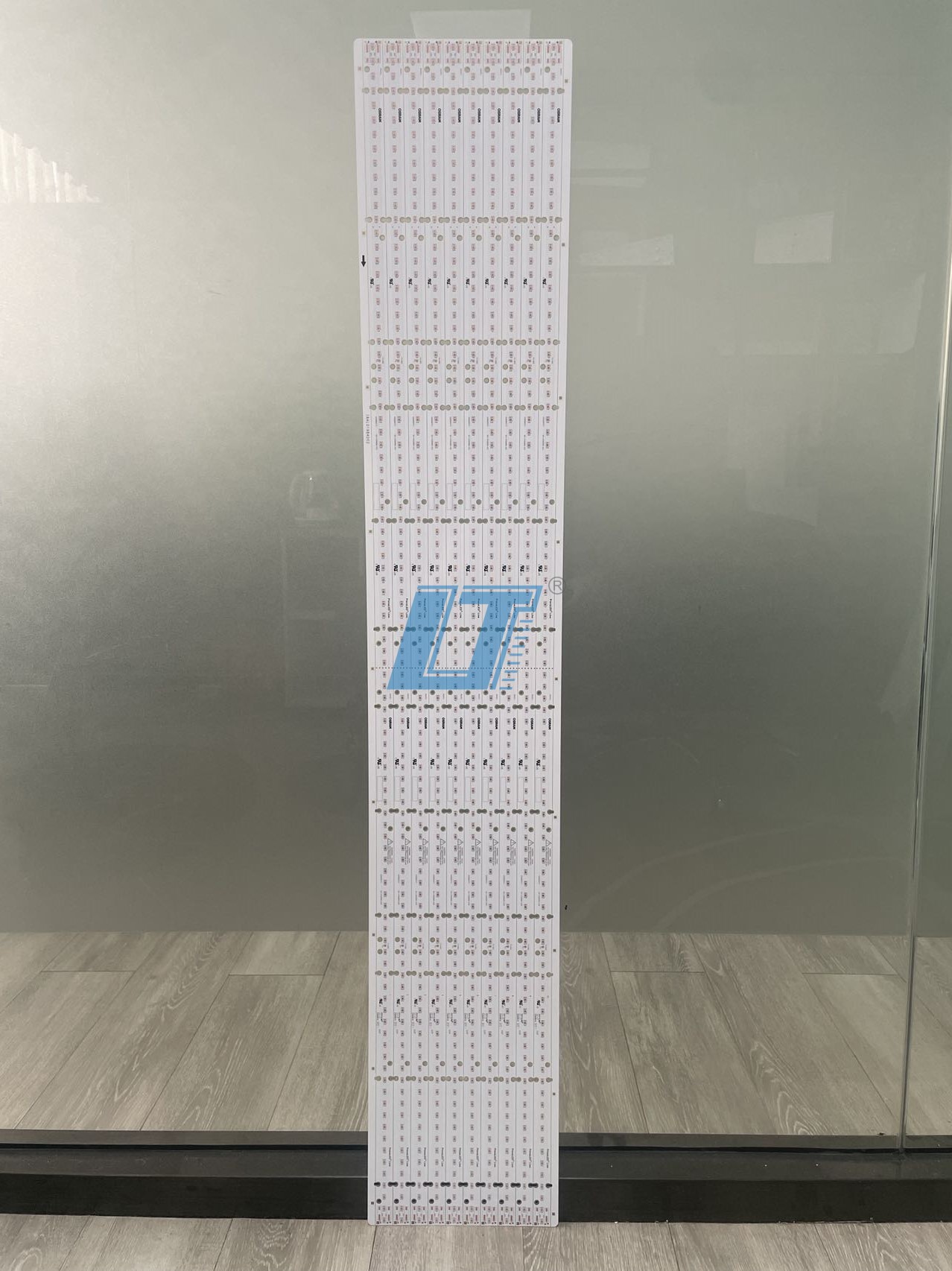
Designing ultra-long-sized multi-layer circuit boards requires a precise and controlled pcb manufacturing process. LT CIRCUIT uses advanced technology and strict quality control to ensure each board meets the highest standards. You will see how each step builds on the last to create reliable, high-performance boards for advanced applications.
Layer Alignment and Lamination
You start with layer alignment and lamination, which are critical for multi-layer boards. Each layer must align perfectly to avoid electrical faults and ensure signal integrity. LT CIRCUIT uses high-precision alignment systems and multi-layer laminating machines. These machines help you achieve consistent results, even with ultra-long-sized boards.
Tip: Accurate layer alignment prevents signal loss and improves board reliability.
Common challenges in this step include interlayer alignment control and pressing process difficulties. You must select the right materials and use advanced positioning methods. LT CIRCUIT collects historical data and applies accurate data compensation to improve alignment. Daily maintenance of the press and careful control of lamination glue and cooling effects also play a role.
Testing Method | Purpose |
|---|---|
Scanning Acoustic Microscopy (SAM) | Identifies layer separation or voids in the laminated part of the circuit board. |
Interconnect Stress Testing (IST) | Assesses interconnection strength under extreme conditions to locate weak areas. |
Solder Float Testing | Reduces the risk of lamination issues during soldering assembly. |
Reflow Simulation Testing | Simulates stresses experienced during soldering to enhance reliability testing. |
You benefit from these controls because they help prevent defects and ensure your board performs as expected.
Drilling and Via Formation
After lamination, you move to drilling and via formation. This step creates the electrical connections between layers. LT CIRCUIT uses both mechanical and laser drilling techniques. Mechanical drilling works well for larger vias, while laser drilling creates precise microvias for high-density interconnects.
Drilling Technique | Description | Applications |
|---|---|---|
Laser Drilling | Uses focused laser beams for precise hole creation, ideal for microvias. | HDI boards, small vias (<75 microns). |
Mechanical Drilling | Traditional method using drill bits, suitable for larger holes. | Larger vias (>75 microns), cost-effective for organic materials. |
You need accurate alignment during drilling to avoid errors. LT CIRCUIT uses specialized machines and markers to align each layer. The company also incorporates thermal vias and metal core layers to help with heat dissipation. Micro via technology allows for hidden wiring, which increases circuit density and improves electrical performance by reducing signal reflection and cross-talk.
Photolithography and Imaging
Photolithography and imaging define the fine circuit patterns on your board. LT CIRCUIT uses advanced LDI (Laser Direct Imaging) machines and laser direct writing technology. These tools expose circuit patterns with high precision, which is vital for ultra-long-sized boards.
The photolithography process includes several key steps:
Clean and condition the copper-clad laminate to prepare the surface.
Apply and cure a liquid photoresist to the cleaned surfaces.
Expose the inner layers using high-precision phototools and UV light.
Develop the exposed layers to reveal the desired circuit pattern.
Etch away unwanted copper, leaving only the intended circuit traces.
Strip the remaining photoresist and treat the copper surface for further processing.
You gain from this process because it ensures sharp, accurate circuit lines and reduces the risk of defects.
Automated Optical Inspection
Automated Optical Inspection (AOI) checks your board for defects after imaging and assembly. LT CIRCUIT uses high-speed AOI systems to scan each board. These systems detect common issues such as solder bridges, shorts, lifted leads, missing components, and misaligned parts.
Defect Type | Detected by AOI |
|---|---|
Solder bridges | Y |
Solder shorts | Y |
Lifted lead | Y |
Missing component | Y |
Misaligned or misplaced part | Y |
AOI improves the yield and reliability of your boards. You see a reduction in defect escape rates by up to 85%. First-pass yield increases from 92% to 98%. Rework costs drop by 60%, and you gain 100% traceability of defects. Most companies achieve a return on investment within eight months.
Note: Automated inspection ensures that only high-quality boards move to the next stage, saving you time and resources.
By following this advanced pcb manufacturing process, LT CIRCUIT delivers ultra-long-sized multi-layer circuit boards that meet the demands of advanced applications. You can trust their expertise and technology to manufacture reliable, high-performance boards every time.
Multilayer PCB Quality and Reliability
Mechanical Stability
You need to ensure mechanical stability in every multilayer circuit board, especially for ultra-long-sized multilayer designs. Mechanical stability affects how well your board withstands stress during both manufacturing and operation. Several factors play a role:
Factor | Description |
|---|---|
Tension imbalances during manufacturing can lead to warping or delamination, requiring precise control. | |
Signal Integrity Over Long Distances | Consistent signal integrity is crucial, necessitating careful impedance matching and trace control. |
Deformation Risks | Flexible designs are prone to deformation, requiring uniform tension during processing to maintain shape. |
Cost Efficiency | Increased length and complexity raise production costs, necessitating advanced design planning. |
Reliability in Demanding Applications | Long-term reliability is essential in critical applications, requiring rigorous testing for durability. |
You can use several testing methods to check mechanical stability during the pcb design process and circuit board manufacturing:
Purpose | Main Failure Modes | |
|---|---|---|
Vibration and Mechanical Shock | Simulates mechanical loads during transportation and operation to verify physical stability. | Cold solder joints, solder ball fatigue, trace cracking |
Thermal Cycling | Simulates thermo-mechanical fatigue stress from temperature changes to assess durability. | Solder joint cracking, delamination, barrel crack |
Damp Heat | Evaluates material stability and electrical insulation under high temperature and humidity. | Moisture absorption, metal migration, blistering |
You should always follow best practices, such as balancing copper distribution and maintaining proper aspect ratios, to prevent warping and delamination in multilayer designs.
Signal Integrity
Signal integrity is a top concern in multilayer circuit board manufacturing. You face several challenges as signals travel long distances across the board:
Faster signal rise times increase signal integrity issues.
High signal frequencies cause signal degradation due to uncontrolled line impedances.
Signal propagation delays can create mismatches in data and clock signals, leading to errors.
Attenuation occurs from trace resistance and dielectric losses, especially at higher frequencies.
Crosstalk between adjacent lines introduces unwanted noise.
Voltage drops in power and ground paths affect device performance.
EMI and EMC issues grow with frequency and faster transitions.
You can address these issues by using proven design strategies:
Strategy | Description | Impact on Signal Integrity |
|---|---|---|
Use advanced laminates with a low loss tangent (< 0.005) instead of standard FR-4 materials. | Reduces signal loss significantly at high frequencies. | |
Copper Foil Selection | Opt for low roughness copper foil to minimize skin effect losses. | Improves signal amplitude by up to 15%. |
Routing Techniques | Avoid running high-speed traces parallel for long distances; increase spacing or insert ground traces. | Reduces crosstalk-induced noise by up to 40%. |
Layer Configuration | Dedicate inner layers to ground and power planes to isolate signal layers. | Ensures cleaner signals in dense designs. |
Via Management | Implement back-drilling to remove unused via stubs. | Reduces signal reflections by up to 25%. |
Differential Pair Routing | Route differential pairs with equal length and consistent spacing. | Maintains signal timing and reduces data errors. |
Simulation and Testing | Use simulation software pre-manufacturing and TDR post-fabrication for verification. | Ensures impedance values are within ±5% accuracy. |
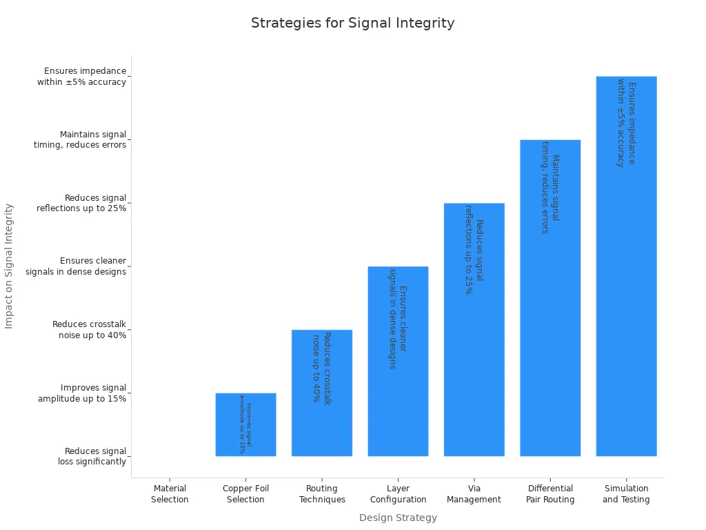
You should validate signal integrity during the pcb design process and prototype testing. LT CIRCUIT uses simulation tools and advanced testing to help you achieve reliable multilayer designs.
Final Testing and Inspection
You must complete thorough testing and inspection to guarantee the reliability of every multilayer circuit board. LT CIRCUIT uses a range of advanced methods:
Testing Method | Description |
|---|---|
Automated Optical Inspection (AOI) | Uses cameras to detect missing parts, incorrect placements, or poor solder joints. |
X-ray Inspection | Inspects hidden joints, such as those under BGAs, to identify internal issues. |
Functional Testing | Tests the completed board to ensure it operates correctly under real-use conditions. |
In-Circuit Testing (ICT) | Checks electrical connections of each component to quickly identify faults. |
Flying Probe Testing | Utilized for small batches, where probes move across the board to test various points. |
You should follow industry standards like IPC-A-600 and IPC-6012 for acceptability and performance. LT CIRCUIT meets or exceeds these standards and holds certifications such as ISO 9001, IATF 16949, ISO 13485, and AS9100D. The company achieves a 99.8% pass rate for aerospace multilayer boards and uses digital twin models and AI analytics for quality assurance.
To ensure long-term reliability, you should:
Maintain aspect ratios below 10:1 for through-hole vias.
Specify adequate annular rings for all layers.
Balance copper distribution to avoid warping.
Expand solder mask around pads to prevent bridges.
Design test points for in-circuit and boundary scan testing.
Validate signal integrity during design and prototyping.
Work with your manufacturer to set test coverage and acceptance criteria.
Apply design for testability principles early in the pcb design process.
Tip: Collaborate with LT CIRCUIT early in your project to benefit from their expertise in multilayer circuit board manufacturing and testing.
You achieve success in ultra-long-sized multi-layer circuit board projects by focusing on advanced stack-up design, careful material selection, and precise manufacturing. Signal integrity and impedance control remain vital for high-speed applications. Partnering with LT CIRCUIT gives you access to expert guidance and reliable technology.
Advanced techniques like photolithography and drilling improve precision.
Design rule checking and DFM analysis help you avoid costly mistakes.
Review your checklist for layout cleanup and manufacturability.
Stay updated on Ultra-HDI technology and evolving PCB standards.
FAQ
What makes ultra-long-sized printed circuit boards different from standard PCBs?
Ultra-long-sized printed circuit boards require special pcb stack-up planning and advanced manufacturing. You must consider mechanical stability, signal integrity, and precise stack-up design. These boards often support high-speed applications and need strict quality control during fabrication and production.
How do you select materials for a reliable pcb stack-up?
You should follow a pcb stack-up design guide. Choose materials with low dielectric loss and matched thermal expansion. This helps prevent warping during manufacturing. LT CIRCUIT recommends using advanced laminates for multi-layer printed circuit boards to ensure durability and performance in demanding applications.
Why is stack-up important in pcb design and fabrication?
Stack-up affects electrical performance, mechanical strength, and manufacturability. You need to plan the stack-up early in pcb design. Proper stack-up design reduces signal loss and improves reliability. LT CIRCUIT uses simulation tools to optimize stack-up for every printed circuit board during fabrication and production.
What testing methods ensure quality in printed circuit board manufacturing?
You can use automated optical inspection, X-ray, and flying probe tests. These methods detect defects in printed circuit boards after fabrication. LT CIRCUIT applies strict testing at every production stage. This ensures each pcb meets industry standards for reliability and performance.
Tip: Always review your pcb stack-up and test coverage before final production. This step helps you avoid costly errors in manufacturing.
See Also
Challenges In Manufacturing And Prototyping Multi-Layer Circuit Boards
Exploring Multilayer PCB Uses In Various Industries
Comprehensive Guide To Heavy Copper Multilayer PCB Production
Understanding The Production Process For Rigid-Flex Circuit Boards
Overcoming Manufacturing Challenges With Buried Via Technology In PCBs