Understanding the Main Challenges of RF Microwave PCB Manufacturing

Manufacturing rf or microwave printed circuit boards differs fundamentally from standard digital board production. At high-frequency, electrical performance depends on material behavior and physical tolerances interacting in ways that standard FR4 boards never face.
You encounter five main challenge categories: material selection, precision control, thermal management, special fabrication processes, and assembly testing. Consider a small etch width variation. That deviation shifts characteristic impedance, which causes insertion loss or signal reflection. Precision sits at the center of understanding main challenges in rf microwave pcb manufacturing.
This article addresses microwave pcb design challenges in practical terms. You will find solutions for rf pcb design and microwave pcb design that reduce risk and improve yield.
Key Takeaways
Choose low-loss materials with stable dielectric constant to minimize signal loss.
Control trace width and spacing tightly to maintain impedance and signal integrity.
Manage heat with thermal vias and copper planes to prevent overheating.
Use plasma etching for PTFE to improve adhesion before plating.
Select immersion silver finish for lowest insertion loss at high frequencies.
Verify impedance with test coupons and TDR on every production panel.
Follow standards like IPC-6018D for reliable RF board manufacturing.
Collaborate early with manufacturers to define tolerances and materials.
Material Challenges in RF Microwave PCB Manufacturing
Laminate choice is the most fundamental decision in rf microwave pcb manufacturing. You cannot correct a poor material selection later in the process. This section sets up the main challenges framework: Dk stability, loss, moisture, cost, and process sensitivity.
Low-Loss Laminate Selection
Controlling Dielectric Constant and Loss Tangent
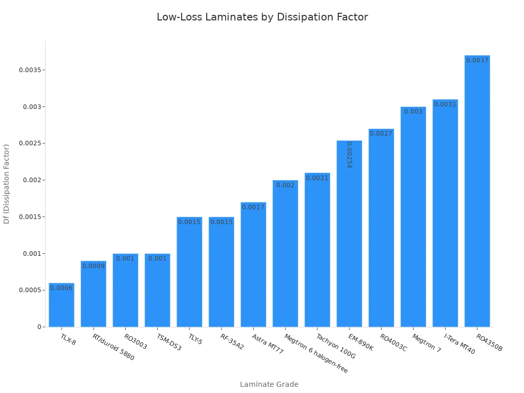
You need rf microwave pcb materials with a low dielectric constant (Dk < 4) and a low dissipation factor (Df < 0.005). These criteria support low signal loss, stable phase, and minimized heat generation at GHz frequencies. Loss tangent scales insertion loss linearly, so values below 0.002 help preserve amplitude in mmWave traces. Stable Dk around 2.1–3.5 reduces size while minimizing variations. Frequency and temperature stability of Dk prevents phase errors in filters.
Balancing Electrical Performance with Cost
PTFE-based laminates like RT/duroid 5880 achieve the lowest electrical loss with Dk of 2.20 and minimal Df. Ceramic-filled composites like RO3003 (Dk 3.00, Df 0.0010 at 10 GHz) provide uniform dielectric properties. Hydrocarbon laminates like RO4350B (Dk 3.48, Df 0.0037) offer a cost-effective balance with FR4-like processability. RF laminates cost 3–5× FR-4 for <10 GHz applications and 8–15× FR-4 for >20 GHz applications.
Substrate Sensitivity and Handling
Moisture Absorption and Dimensional Stability
PTFE materials generally have low moisture absorption, which is essential for maintaining electrical performance and dimensional stability in humid environments. PTFE-based laminates show very low moisture absorption (<0.1%). However, PTFE-ceramic composites may have slightly higher moisture absorption compared to other PTFE types. You should consider this for applications in high-moisture conditions.
Surface Preparation for PTFE and Soft Materials
PTFE requires specialized drilling and lamination. Pure PTFE has high CTE (~160 ppm/°C) requiring fillers for rigidity. RT/duroid 6002 (Dk 2.94) specifically addresses pure PTFE's poor dimensional stability by closely matching copper CTE. This ensures plated-through-hole reliability in high-layer-count aerospace boards.
Process Control for Consistent Materials
Managing Panel-to-Panel Variation
Ceramic-filled PTFE composites improve Dk stability. RO3000 series laminates maintain consistent mechanical properties across different Dk values, preventing warpage in mixed-Dk multilayer boards. RO4003C and RO4350B are manufactured with tight Dk control and low loss. The RO4000 series has a low temperature coefficient of Dk, reducing Dk drift with temperature.
Collaborating Across Design, Materials, and Fabrication
Begin with the frequency and loss budget to narrow material properties. Simulate impedance using vendor models, targeting 50-ohm lines. Specify Dk and Df at the operating frequency and temperature for accuracy. Verify with test coupons per standard methods during qualification to ensure simulation-to-hardware correlation.
Microwave PCB Design Challenges: Precision and Tolerances
In microwave pcb design, physical deviations decide success. Trace width, spacing, and registration shift performance. Understanding main challenges in rf microwave pcb manufacturing begins here. Specify geometry before layout.
Understanding Main Challenges in Impedance Control
Etch Tolerances and Line-Width Control
Trace width accuracy is your first defense. In microwave pcb design challenges, a ±1 mil change can shift characteristic impedance. Most fabricators hold controlled impedance traces within ±10%. Keep trace spacing at least three times the dielectric thickness.
Tighter tolerance requires more process control. You cannot write ±3% on a drawing and expect it everywhere. Define which nets need control. This defines quality fabrication practice.
Impedance Verification with Coupons and TDR
You verify characteristic impedance using test coupons on every panel. Coupons replicate the trace geometry and stack-up. TDR verification presents microwave pcb design challenges. A fast-rise-time step signal reveals impedance.
Standard tolerance is ±10%; precision designs achieve ±5%. TDR data shows measured impedance, target values, and pass/fail status for each coupon, confirming signal integrity. You receive insertion loss via S-parameter measurement for microwave pcb layout design.
Layer Stack-Up and Registration Control
Optimizing Stack-Up for Signal Integrity
Your pcb stack-up determines signal integrity before routing. In microwave pcb design, assign solid power and ground planes as adjacent internal layers. Impedance-controlled traces require known dielectric thickness. Route traces orthogonally.
Keep signal traces shorter than one twentieth of the wavelength for signal integrity. Consider the 20H rule for high-frequency RF. A pcb stack-up is the backbone of microwave pcb design. These choices belong to rf pcb design and manufacturing.
Compensating Substrate Shrinkage in Multilayer Boards
During lamination, dielectric materials expand. Pads shift from their designed positions. Fabricators counter this with board scaling: enlarge inner layers before lamination; the board shrinks back to exact dimensions. This is essential in microwave pcb design.
Internal target fiducials track material movement. Laser direct imaging scales each panel. X-ray inspection updates shrinkage predictions. For an 18 by 24-inch eight-layer board, layer two and three may expand 0.014 inches on the long axis and 0.012 on the short. This is a microwave pcb design challenge.
Crosstalk, Shielding, and EMI Sensitivity
Spacing, Ground Planes, and Isolation
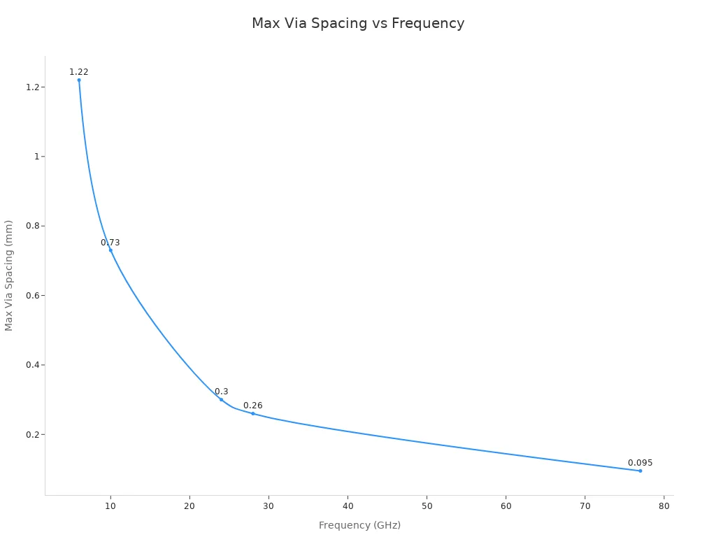
Crosstalk rises when traces are close. Apply the 3W rule: spacing at least three times trace width. Via spacing matters at high-frequency: at 6 GHz, via spacing is 1.22 mm; at 24 GHz, 0.30 mm.
Double-row via fences push isolation above 40 dB. Offset the second row by half the pitch. This poses rf pcb design challenges. Keep via-to-trace clearance at least three times trace width. Every via adds parasitic capacitance.
Shielding Approaches for High-Frequency Circuits
Shielding requires a cage, not isolated vias. Wrap via fences around ninety-degree bends. Close the cage at both ends. In multilayers, stitch ground planes every one to two millimeters at 10 GHz. Managing crosstalk is one of the microwave pcb design challenges.
Surface-mount components avoid parasitic inductance. Beryllium copper gaskets maintain shield effectiveness at seams. The chart below shows via spacing falling as frequency climbs. These practices belong to rf pcb design.
Thermal Challenges in RF PCB Design
Heat decides reliability on power-dense boards. RF power amplifiers dissipate 40–70% of DC input power as heat, and typical efficiency sits between 30–60%. Without adequate cooling, junction temperatures exceed safe limits. Every 10°C rise in junction temperature roughly halves expected device lifetime. Excessive heat also lowers gain, raises noise, and drifts frequency. These are the rf pcb design challenges you cannot route around.
High-Power Density and Heat Spreading
Thermal Vias and Copper Plane Design
Thermal via arrays create low-resistance vertical paths beneath exposed thermal pads. A single 0.3 mm plated via through 1.6 mm FR4 shows roughly 192°C/W per IPC-2221B. A copper-filled via drops that to about 59°C/W, and a 5×5 array of copper-filled vias approaches 2.4°C/W. A 10W device targeting 2°C/W needs roughly 30 vias; IPC-2152 recommends one via per 0.5–1 mm² of thermal pad area. Keep via pitch at 0.8 mm or more and aspect ratio below 10:1 per IPC-4761.
Copper planes then spread heat horizontally. Connect the via array to internal ground and power planes to cut effective thermal resistance by 20–50% versus an isolated array. Copper coin structures suit vertical heat transfer beyond the limits of via arrays and heavy copper alone.
Heatsinking and Grounding Strategies
High power density often exceeds natural convection. You move to conduction, forced air, liquid cooling, or heat pipes. Liquid cooling serves very high power density. GaN-on-SiC technology offers superior thermal conductivity and reliability at elevated temperatures. Heat sinks, spreaders, thermoelectric coolers, and copper coins all transfer heat to a chassis or cold plate.
CTE Mismatch and Board Warpage
Preventing Plated Through-Hole Cracks
Copper expands at about 16–17 ppm/°C in-plane, while laminates vary: FR-4 at 14–17, RO4350B at 10–14, and RO3003 at 7–9 ppm/°C. That difference stresses the copper-laminate interface and can crack plated through-holes. Choose laminates with CTE close to copper. IPC-2228 gives sectional guidance for RF/microwave board design. Balanced copper distribution, enlarged annular rings, teardrop transitions, staggered vias, and materials with Tg above 170°C all reduce cracking risk.
Reducing Warpage During Lamination and Assembly
Asymmetric CTE across the neutral axis bows the board during cooling. A 10 ppm/°C in-plane imbalance between upper and lower halves typically bows a 200 mm board by roughly 0.5–1 mm. A symmetric, mirrored stack-up cancels that bending. Asymmetry amplifies it. This is a core microwave pcb design challenge.
Thermal Simulation for RF/Microwave Boards
Modeling Hotspots in Power Amplifier Circuits
Junction temperature equals ambient temperature plus dissipated power multiplied by total thermal resistance. Model hotspots before layout. Simulation reveals where via arrays, copper weight, or coins are needed.
Selecting Thermally Conductive Dielectric Materials
Material choice sets the thermal ceiling. Ceramic-filled and hydrocarbon laminates handle heat better than standard FR4. Match the dielectric to the power level and cooling method. Understanding main challenges here means treating thermal design as a first-class requirement in rf pcb design, not an afterthought.
Special Process Requirements for RF PCBs
RF and microwave boards demand processes that standard FR4 fabrication never touches. Surface activation, PTFE bonding, and via stub control separate high-frequency pcb fabrication from ordinary board work. These steps define common issues in rf pcb manufacturing.
PTFE Surface Preparation and Bonding
Plasma Etching and Chemical Activation
PTFE resists adhesion naturally. Plasma etching solves this by cleaving strong carbon-fluorine bonds and introducing polar oxygen groups. This makes the inert surface wettable and chemically receptive to plating. The same action creates microscopic roughness for mechanical interlocking.
XPS measurements show the fluorine-to-carbon ratio drops from about 2.0 in virgin PTFE to as low as 0.2 after plasma exposure. Optimal treatment yields roughly 1.0–1.2 N/mm peel strength with cohesive failure inside the PTFE. Under-treatment gives about 0.8 N/mm; over-treatment drops below 0.5 N/mm. For pure PTFE, use a CF4/O2/N2 mixture at 300–500 W RF power, 100–200 mTorr, and 8–12 minutes. Plate within 12 hours to preserve the activated surface.
Bonding Film Selection and Press Cycles
PTFE materials like RO3003 and RT5880 cannot bond with standard FR4 prepreg. You need specialized films such as Rogers 2929 bondply or low-flow alternatives like LD621. PTFE-containing stackups are limited to 2 press cycles total. Each cycle introduces layer shift risk, so more cycles mean tighter registration tolerance.
Drilling, Plating, and Via Stub Control
Hole Wall Quality for Reliable Plating
PTFE and ceramic-filled materials require adjusted drill parameters to prevent smear. Plasma treatment uses different gases than standard FR4 boards. Inadequate hole prep leads to poor copper plating and unreliable interconnections. Ceramic-impregnated laminates are hard on drill bits, requiring reduced hit counts and customized spindle speeds. V-scoring is generally not recommended because saw blades can tear material and pull copper from the surface.
Back-Drilling to Remove Unwanted Stubs
Back-drilling removes the unused copper portion of a via, called the via stub. In high-frequency circuits, a stub acts like an antenna and creates resonant effects that absorb and reflect signal. These resonances increase insertion loss and distort transmission. Shortening or eliminating the stub reduces these effects and improves signal integrity.
Surface Finishes for High-Frequency Reliability
ENIG, ENEPIG, and Immersion Silver Options
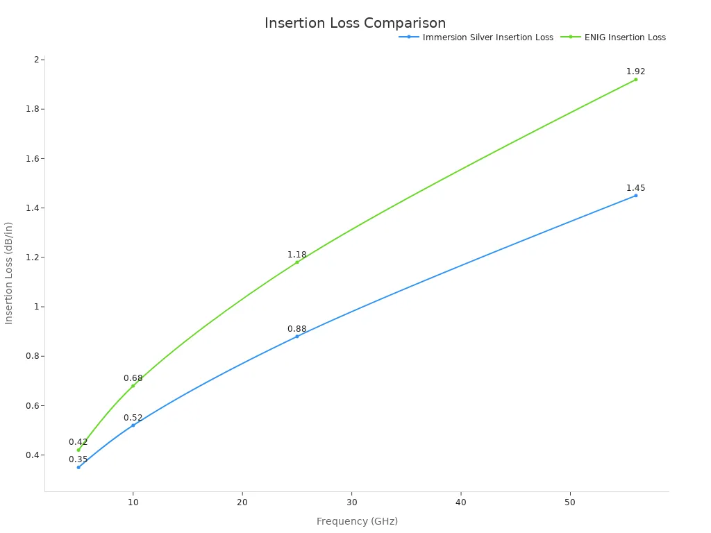
At high frequencies, RF current flows in a thin skin layer at the conductor surface. At 10 GHz, skin depth in copper is approximately 0.66 µm. Nickel has much lower conductivity, so ENIG's nickel layer increases pad resistance and insertion loss above roughly 1–2 GHz. Immersion silver deposits directly on copper with no nickel barrier, giving the lowest finish-related loss. ENEPIG adds palladium for wire bonding and eliminates black pad risk.
Controlling Finish Thickness for Insertion Loss
Finish thickness directly affects loss. At 25 GHz, immersion silver shows 0.8–1.0 dB/in while ENIG shows 1.1–1.4 dB/in. At 56 GHz, immersion silver reaches 1.45 dB/in versus ENIG at 1.92 dB/in. Immersion silver offers excellent coplanarity and lower cost, but shelf life is shorter at 6–12 months sealed. ENIG provides 12+ months shelf life and broader supplier availability.
Assembly and Testing in RF PCB Manufacturing
Assembly and test expose every weakness from material and precision stages. A high-frequency board fails at the interconnection when placement, solder, or finish is inconsistent. These manufacturing issues demand disciplined process control.
Component Assembly and Reliability
Placement Accuracy and Solder Joint Integrity
Soft PTFE substrates create placement problems. Pick-and-place pressure can dimple the surface, misalign fiducials, and shift SMD components. These offsets cause head-in-pillow defects, open joints, or solder bridges after reflow. Low surface energy also reduces solder paste adhesion.
Inaccurate placement increases insertion loss, creates impedance discontinuities, and introduces EMI. Parasitic effects from vias, pads, and traces compound the problem. X-ray inspection measured 14.08% voiding in a solder joint, which still met IPC-7095 Class 3. This shows how you verify solder reliability during rf microwave pcb manufacturing.
Mechanical Concerns: Board Weight and Handling
Heavy copper planes and metal-backed substrates add weight. You need fixtures that support the board during assembly. Handling procedures must prevent flexing, which cracks brittle ceramic-filled laminates.
Testing High-Frequency Performance
Vector Network Analyzer (VNA) Measurements
VNA testing confirms insertion loss and return loss. You select a calibration method based on your test setup. SOLT uses known short, open, load, and through standards. TRL assumes constant port match. Ecal characterizes a test port with a single connection.
Before calibration, verify the frequency range and inspect cables for damage. Constrain cables in a fixed position. Cable movement during calibration degrades measurements, especially at high-frequency. Reduce IF bandwidth from 35 kHz to 500 Hz for accuracy. Avoid smoothing because it masks real response features.
Time-Domain Reflectometry and Test Coupons
TDR verification uses test coupons on every panel. A fast-rise-time step signal reveals impedance. Standard tolerance is ±10%; precision designs achieve ±5%. You receive pass/fail status for each coupon.
Quality Control and Regulatory Compliance
Automated Inspection Methods for RF Boards
Automated optical inspection catches surface defects. X-ray inspection verifies solder voiding beneath thermal pads. You combine both methods for complete coverage.
Meeting Reliability Standards and Documentation
Standards depend on your application. IPC-6018D covers microwave/RF PCBs with tight tolerances on via plating and conductor width. MIL-PRF-31032 adds shock, vibration, and qualification lot testing for defense work. IPC Class 3 demands zero-defect acceptance for critical features like high-frequency transmission lines.
Our rigorous testing and adherence to internationally recognized quality and environmental standards are just a few reasons why TTM's teams are recognized as exceptional and why leading brands worldwide trust our advanced technology solutions.
Documentation includes full traceability, detailed test reports, and complete transparency. ISO 9001:2015, UL approval, RoHS compliance, and ITAR registration support rf pcb design and manufacturing for regulated markets. These requirements shape rf pcb design from the start. Successful rf and microwave pcb projects depend on close collaboration between designers and manufacturers. You must define material and tolerance requirements early, choose an experienced partner, and match test strategies to your frequency range. rf circuit boards will only face tighter tolerances as frequencies climb.
Material selection drives process behavior and thermal reliability. Precision requirements shape test complexity. Assembly demands hold everything together. These forces tie microwave pcb design to manufacturing reality, creating microwave pcb design challenges at every step.
Start collaboration early. Front-to-back registration (±0.002 in) and trace-width tolerances (±0.05 mm) demand it. Hybrid stack-ups, combining FR4 with PTFE, balance performance and cost. At 30 GHz, shield openings must stay under 1 mm. High-frequency designs tighten every tolerance.
Define material and tolerance requirements first. Choose an experienced rf pcb design and manufacturing partner. Match test strategies to your frequency range. These best practices for rf pcb design turn understanding main challenges into solutions for rf pcb design challenges.
FAQ
How tight does trace-width control need to be for RF boards?
Most fabricators hold controlled impedance traces within ±10%. Precision designs reach ±5%. A ±1 mil change shifts characteristic impedance noticeably. You should specify critical nets only. Tight tolerances across every trace raise cost without improving performance.
Why does PTFE require plasma etching before plating?
PTFE resists adhesion because of strong carbon-fluorine bonds. Plasma etching cleaves those bonds and adds polar oxygen groups. The surface becomes wettable and microscopically rough. XPS shows the fluorine-to-carbon ratio drops from about 2.0 to 0.2 after exposure. Optimal peel strength reaches roughly 1.0–1.2 N/mm.
How does via spacing change with operating frequency?
Via spacing must shrink as frequency rises. At 6 GHz, maximum via spacing sits near 1.22 mm. At 24 GHz, it drops to 0.30 mm. At 77 GHz, shielding demands even tighter pitch. Use double-row via fences to push isolation above 40 dB.
Which surface finish gives the lowest insertion loss?
Immersion silver gives the lowest finish-related loss because it deposits directly on copper. At 25 GHz, immersion silver shows 0.8–1.0 dB/in versus ENIG at 1.1–1.4 dB/in. At 56 GHz, the gap widens further. ENIG costs more and adds nickel loss. Choose silver for performance, ENIG for shelf life.
What causes plated through-hole cracks in RF boards?
CTE mismatch between copper and laminate stresses the barrel during thermal cycling. Copper expands at 16–17 ppm/°C. RO3003 expands at 7–9 ppm/°C. Choose laminates with CTE close to copper. Use Tg above 170°C, balanced copper, and teardrop transitions to reduce crack risk.
How do you verify impedance on a production RF panel?
You use test coupons on every panel. TDR sends a fast-rise-time step signal through the coupon and reveals impedance. Standard tolerance is ±10%; precision designs achieve ±5%. The report includes measured impedance, target values, and pass/fail status for each coupon.
What documentation matters for defense or aerospace RF boards?
IPC-6018D covers microwave/RF PCBs with tight tolerances on via plating and conductor width. MIL-PRF-31032 adds shock, vibration, and qualification lot testing. IPC Class 3 demands zero-defect acceptance for high-frequency transmission lines. Keep full traceability, test reports, and material certifications.
