Understanding Vertical Continuous Plating in Achieving Copper Thickness Tolerance
Vertical continuous plating delivers consistent copper thickness across printed circuit boards, which directly improves pcb reliability and performance. Industry standards demand tight copper thickness tolerance, as even a 10% variation can affect heat dissipation and impedance. LT CIRCUIT uses advanced plating technology to ensure quality and precision in every pcb they produce.
Key Takeaways
Vertical continuous plating ensures uniform copper thickness on PCBs, which improves their reliability, heat management, and electrical performance.
LT CIRCUIT uses advanced plating technology and strict quality control to deliver high-quality PCBs with precise copper thickness and fewer defects.
Vertical plating offers faster production, better copper distribution, and stronger boards compared to traditional methods, making it the future of PCB manufacturing.
Vertical Continuous Plating in PCB Manufacturing
Copper Thickness and PCB Quality
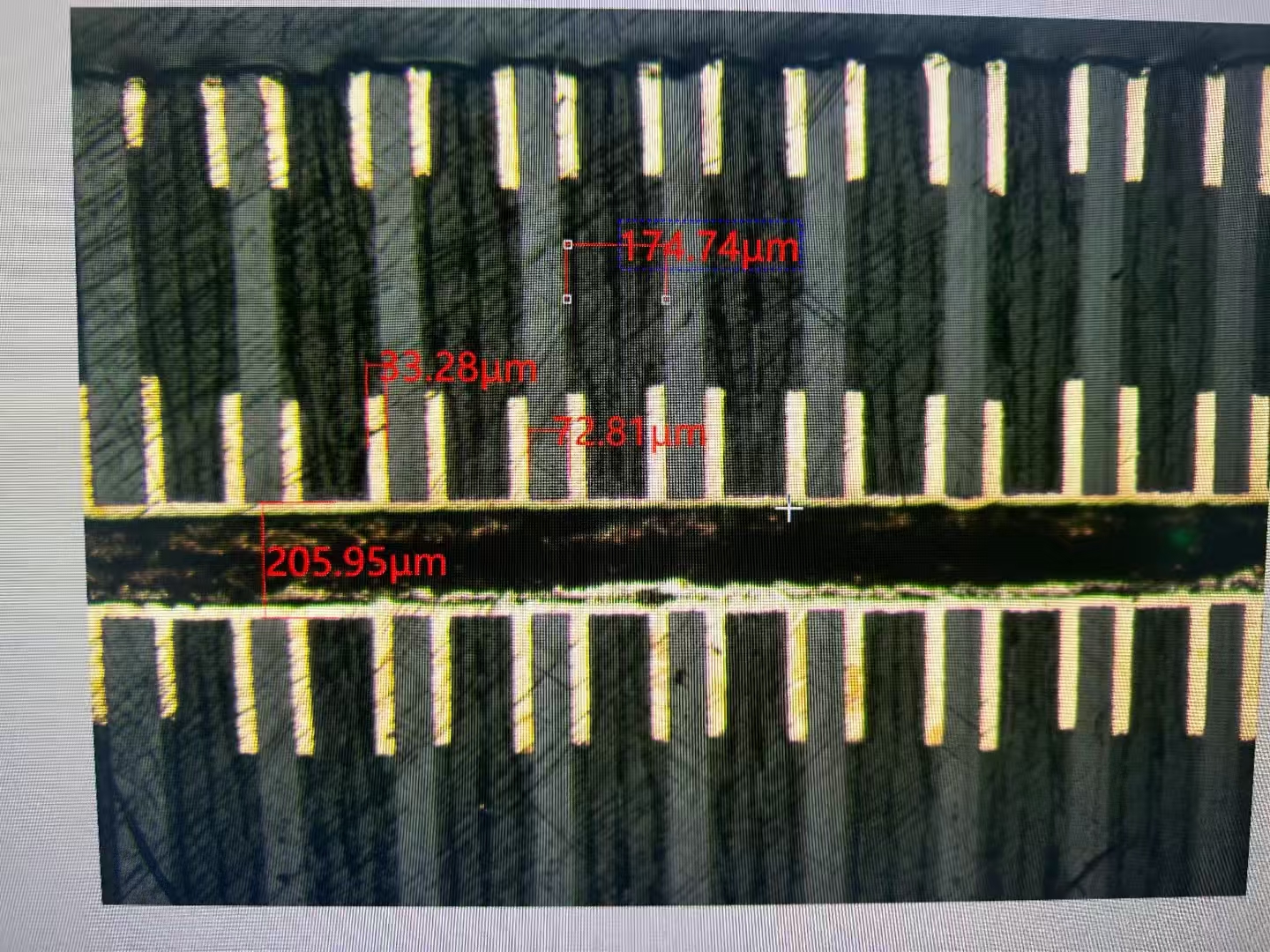
Copper thickness plays a vital role in the performance and reliability of every pcb. Uniform copper thickness ensures that each board can handle electrical currents safely and efficiently. Research shows that even small differences in copper thickness can lead to problems such as poor heat dissipation or signal loss. Studies using simulations and experiments confirm that uniform copper thickness improves the overall quality of pcbs by reducing the risk of adhesion failures and increasing mechanical strength. When copper thickness remains consistent, the copper plating process creates stronger bonds between copper and the substrate, which helps prevent delamination and other defects.
The copper plating process also affects the surface quality of the copper layer. A smooth and even copper surface improves the wettability and mechanical interlocking with the board’s materials. This leads to better performance and longer lifespan for the pcb. Manufacturers who control copper thickness can deliver boards that meet strict industry standards for reliability and durability.
Process Overview
The vertical continuous plating process uses advanced techniques to achieve precise copper thickness across all areas of the pcb. The process begins with careful pretreatment of the board surface, including oil removal and charge adjustment. This step prepares the board for the copper plating process and ensures good adhesion.
The plating process continues with strict control of bath parameters. Operators adjust the temperature to increase the diffusion rate of copper ions, which helps achieve a uniform copper layer. The plating solution flows quickly and consistently through vias and holes, forming a thin diffusion layer that is critical for even copper distribution. Multiple nozzles in the vertical copper plating system create vortex convection, which further reduces the diffusion layer thickness and improves copper plating uniformity.
Note: The use of advanced additives such as accelerators, suppressors, and levelers in the copper plating process helps regulate the deposition rate and surface smoothness. These additives, combined with techniques like reverse pulse current plating and ultrasonic vibration, ensure that copper fills vias evenly and prevents defects such as dog-boning.
Engineers also use conductive rollers and proper cathode arrangements to maintain consistent current distribution during the plating process. This attention to detail results in flatter and more balanced copper deposits, which are essential for high-density interconnect and multilayer pcb manufacturing.
LT CIRCUIT’s Approach
LT CIRCUIT uses state-of-the-art vertical continuous plating technology to deliver high-quality pcb products. The company’s copper plating process relies on high throwing power acid copper baths that operate at modern current densities. These baths, combined with organic additive packages and eductor agitation, produce bright, ductile copper deposits with excellent mechanical properties. The copper plating process achieves a microdistribution of about 85% for aspect ratios as high as 8:1, supporting advanced printed circuit board production.
LT CIRCUIT’s quality control system uses cyclic voltammetric stripping to monitor and adjust plating additives, ensuring consistent copper thickness and deposit quality. The vertical copper plating equipment features insoluble anodes, which eliminate nodulation and stabilize the anode area. This design improves the consistency of copper plating and reduces the risk of defects.
The company’s engineers optimize every step of the copper plating process, from pretreatment to final inspection. They address challenges such as reverse flow and tip effects at via entrances, which can cause uneven copper thickness. By adjusting process parameters and using advanced chemistries, LT CIRCUIT ensures that every pcb meets strict requirements for copper thickness, distribution, and reliability.
Vertical Copper Plating vs. Traditional Methods
Process Differences
Vertical copper plating stands out from traditional horizontal and rack plating methods in several ways. In vertical copper plating, each pcb panel moves through the plating process individually. This approach allows for precise control over copper thickness and distribution, especially in complex via structures. Traditional horizontal plating often uses batch processing, which can lead to uneven copper plating and less control over thickness. The vertical plating process uses advanced bath compositions and additives, such as dispersants and grain refiners, to achieve uniform copper deposits. The table below highlights some technical differences:
Aspect | Vertical Copper Plating | Traditional Plating Methods |
|---|---|---|
Current Density | Lower (4-8 A/dm²) | |
Process Orientation | Vertical, continuous | Horizontal or rack-based |
Additives | Specialized for uniform copper distribution | Standard, less optimized |
Defect Mitigation | Focus on via filling and defect reduction | Less emphasis on high-speed defect control |
Product Quality | Uniform, dense copper plating | Standard, may vary across boards |
Quality and Efficiency
Vertical copper plating improves both quality and efficiency in pcb manufacturing. The process eliminates extra steps like tin application and stripping, which streamlines production. Each pcb receives individual attention, resulting in more consistent copper thickness and better copper plating distribution. This method reduces the risk of defects in via filling and ensures stronger copper bonds. Key benefits include:
Faster production times and shorter lead times
Fewer process steps, reducing the chance of errors
Flatter, more uniform copper plating across all boards
Enhanced quality control for each pcb
Manufacturers like LT CIRCUIT use vertical copper plating to meet strict industry standards. Their advanced plating process supports high-density via structures and ensures reliable copper plating for every pcb.
Industry Trends
The pcb industry continues to shift toward vertical copper plating due to its clear advantages. Companies now focus on automation, real-time monitoring, and data-driven quality control. Vertical copper plating systems use robotics and IoT devices to track the plating process and maintain copper thickness. These systems also support closed-loop recycling, which saves energy and reduces waste. As demand for high-performance boards grows, vertical copper plating helps manufacturers deliver consistent copper plating and reliable via filling. LT CIRCUIT leads this trend by adopting vertical copper plating technology, ensuring every pcb meets modern requirements for copper thickness, distribution, and quality.
Vertical continuous plating gives every pcb consistent copper thickness.
LT CIRCUIT leads the industry with advanced plating for high-quality pcb production.
The future of pcb manufacturing will see more companies use vertical plating to improve reliability and performance.
Customers can expect better pcb results with this technology.
FAQ
What is vertical continuous plating?
Vertical continuous plating is a process that coats PCBs with copper in a vertical orientation. This method ensures even copper thickness and high-quality results.
Why does copper thickness matter in PCBs?
Copper thickness affects electrical performance and heat management. Uniform copper layers help PCBs last longer and work more reliably.
How does LT CIRCUIT ensure copper thickness tolerance?
LT CIRCUIT uses advanced equipment and real-time monitoring.
Engineers check copper thickness at every stage for consistent quality.
See Also
Impact Of Vertical Continuous Electroplating On Copper Thickness Uniformity
Utilizing Horizontal Copper Sinking Methods In PCB Manufacturing
Importance Of Gantry Electroplating Lines For Half-Hole PCB Copper
Techniques To Achieve Flat Electroplated Filling Holes In HDI PCBs
Using Panasonic Copper-Clad Laminates For Advanced PCB Production