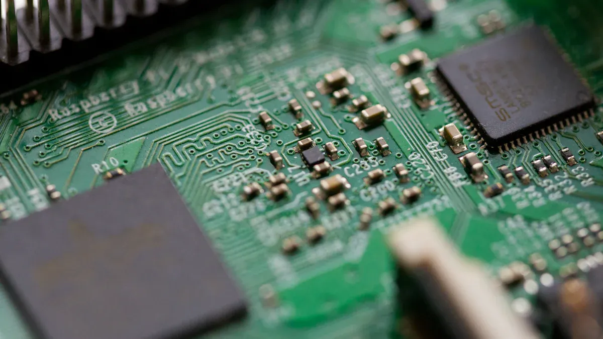
What Are High-Speed PCBs

High-speed PCBs are special boards for fast signals and data. They help keep signals clear so devices work well. Without them, problems like weak signals or timing issues can happen. These boards also cut down on signal interference, making electronics work better. For things like 5G or advanced computers, they are key for smooth and accurate communication.
Key Takeaways
High-speed PCBs are important for fast digital devices. They keep signals clear and lower interference, which helps 5G and modern computers work well.
Making high-speed PCBs needs good planning. Using methods like impedance control and smart routing keeps signals strong and improves how they work.
Picking the right materials matters for high-speed PCBs. Materials that lose less signal improve quality and handle heat better, making devices last longer.
Why High-Speed PCBs Are Important in Modern Electronics
Role of High-Speed PCBs in Fast Digital Systems
High-speed PCBs are key for fast digital systems. They help signals move quickly and correctly across the board. In high-speed systems, keeping signals clear is very important. These boards handle signals above 50 MHz, where small mistakes can cause big problems.
"The layout of high-speed PCBs is very important. These boards handle signals over 50 MHz and need impedance control to reduce signal loss."
To make this work, designers use methods like controlling impedance, placing ground planes well, and keeping signal paths short. These steps lower signal loss and stop interference. For example, putting ground planes near signal paths keeps impedance steady. It also gives signals a clear return path, cutting noise and improving power and signal quality.
"Routing high-speed PCBs needs ground planes near signal paths. This keeps impedance steady and ensures good signal and power quality."
By solving these problems, high-speed PCBs make systems faster, more reliable, and able to handle tough tasks.
Uses in Advanced Technology (like 5G, IoT, and Computers)
High-speed PCBs are vital for advanced tech like 5G, IoT, and computers. These need fast data, low delays, and strong performance, which high-speed PCBs provide.
In 5G, these boards support high-frequency signals and reduce signal loss for smooth communication. IoT devices use small, low-power boards for wireless tasks. Computers rely on high-speed PCBs for faster processing and better data transfer.
Application Area | Key Needs |
|---|---|
Cars | Strong signal control, good heat management |
Entertainment Systems | Compact designs, support for multimedia |
Factory Machines | Long-lasting, reliable, and tough in harsh conditions |
Internet of Things | Small, low-power boards for wireless and long battery life |
These examples show how high-speed PCBs meet the needs of different industries, ensuring great performance.
Benefits of High-Speed PCB Design for Better Performance
High-speed PCB design brings many benefits for better performance and reliability. Using special materials and careful building methods improves signal quality and heat control. For example, ultra-low loss materials cut signal loss by over 6 dB at 2.5 GHz, boosting performance.
Material Type | Signal Loss at 2.5 GHz | Performance Boost |
|---|---|---|
Regular Material | 1 dB | Small Improvement |
Medium-Loss Material | 2 dB | Moderate Improvement |
Ultra-Low Loss Material | >6 dB | Big Improvement |
High-speed PCBs also reduce interference and keep signals steady, which is crucial for telecom and medical tools. They manage heat well, letting devices work even in tough conditions.
"Good signal quality needs smart planning. Short signal paths help avoid interference and improve performance."
By using high-speed PCB design, you can build faster, stronger, and longer-lasting systems that meet today’s tech demands.
Key Challenges in High-Speed PCB Design
Signal Integrity and Noise Management
Keeping signals clear is very important in high-speed PCBs. Signals can get messed up by noise, crosstalk, or EMI (electromagnetic interference). This can cause devices to work poorly. Crosstalk happens when a signal in one wire affects a nearby wire. This can mess up paired signals, especially in fast data systems.
To handle noise, tools like oscilloscopes and jitter analyzers are helpful. These tools check for timing errors and help fix them. Also, routing traces with the right impedance reduces signal bounce and keeps signals clean.
About 1.5% noise can affect nearby wires in high-speed designs. If a signal runs at 3.3 V with a noise limit of +/- 300 mV, this noise level is okay. But too much noise can ruin the signal.
Using methods like pairing wires and matching their lengths helps. It makes sure signals arrive together, reducing timing problems and making systems more reliable.
Impedance Control and Crosstalk Mitigation
Impedance mismatches can cause signals to bounce back, leading to errors. To stop this, match the impedance of the source, receiver, and traces. This keeps signals smooth and avoids data loss. In fast PCBs, even small mismatches can cause big problems.
To reduce crosstalk, space out traces and plan their paths carefully. Keeping traces farther apart lowers interference. Ground planes also help by giving signals a steady base and keeping impedance stable.
Technique | Description |
|---|---|
Match source, receiver, and trace impedances to avoid signal bounce. | |
Differential Pair Routing | Keep paired wires close in length for better timing. |
Via Optimization | Shorten via stubs and improve return paths to reduce signal loss. |
Power Integrity Management | Use capacitors and good power paths for steady power. |
EMI Mitigation | Control signal edges and use shields to cut interference. |
Simulation and Validation | Test designs before and after building to fix signal issues. |
For example, a server motherboard had errors in DDR4 memory due to timing issues. Fixing the trace lengths and improving the ground plane solved the problem. This shows how important it is to match trace lengths and plan routes well in high-speed PCBs.
Material Selection for High-Frequency Applications
Picking the right materials is key for high-speed PCBs. Fast systems need materials with steady properties to avoid signal problems. Materials that absorb less water stay stable longer.
Heat control is also important. Materials that spread heat well work better in powerful devices. For example, IT-968 handles heat better than IT-988G, making it great for tough jobs.
In thin circuits, conductor losses matter more than material losses. Using low-loss materials keeps signals strong and improves performance. Also, the glass transition temperature (Tg) shows how well a material holds up under heat.
Tip: Choose materials with low signal loss, good heat control, and steady properties. These features keep high-speed PCBs working well in advanced systems.
By choosing the right materials and improving their features, you can make high-speed PCBs that are reliable and work well in modern technology.
Essential Tips for High-Speed PCB Design with LT CIRCUIT
Planning Layers and Stack-Up
Good layer planning is key for high-speed PCBs. Arrange layers carefully to keep signals clear and manage heat. For example, placing signal layers near ground planes reduces signal loss. It also gives signals a steady return path. Balanced stack-ups stop boards from bending during production, making them more reliable.
Studies show how important layer arrangement is. For instance:
Time | Session Title | Key Topics Covered |
|---|---|---|
10:00 a.m. to 3:00 p.m. | Beyond the Layers: Advanced Techniques for PCB Stack-Up Design | Impedance control, signal integrity, thermal considerations, and real-world examples of effective strategies. |
By following these tips, you can make PCBs that are fast and durable.
Routing High-Speed Signals
Routing high-speed signals needs careful planning. Avoid sharp 90-degree corners because they mess up signals. Use smooth curves or 45-degree angles instead. Matching trace lengths is also very important. For paired signals, keep trace lengths close, within 5-10 mils, to avoid timing problems.
Here are some helpful routing tips:
Match trace lengths for paired and parallel signals.
Use copper pours and thermal vias to handle heat.
Use tools like Ansys HFSS to check signal quality.
These steps help your PCB handle data quickly and reliably.
Reducing Interference in Layouts
Cutting interference is very important in high-speed PCBs. Ground planes help block electromagnetic interference (EMI). Overlapping ground planes at key spots lowers noise and crosstalk.
Some useful techniques include:
Keeping ground planes continuous to stop signal reflections.
Adding ground vias to improve stability.
Reducing loop areas to lower EMI in high-speed designs.
Tests show that continuous ground planes make signals much clearer. By using these methods, you can design PCBs that work fast and perform well.
High-speed PCBs are important for today’s electronics. They help send data quickly and keep systems working well. Careful design solves problems like signal clarity and impedance issues. Check out LT CIRCUIT’s smart ideas to build strong PCBs for modern tech needs.
FAQ
What makes high-speed PCBs special compared to regular ones?
High-speed PCBs work with fast signals and high frequencies. They use better materials and smart designs to keep signals clear and cut down interference.
How do you keep signals strong in high-speed PCB design?
You use methods like matching impedance, adding ground planes, and shortening signal paths. These steps lower noise and make signals better.
Can LT CIRCUIT create custom high-speed PCBs for specific uses?
Yes! LT CIRCUIT makes custom PCBs for telecom, IoT, and computers. Their designs fit your needs perfectly. 🚀
See Also
Understanding High-Speed PCB Design And Its Importance
Manufacturing High Frequency PCBs For RF Design Needs
Guide To Production Technologies For Heavy Copper PCBs