What Is a Multilayer RF PCB and How Does It Work

You use a multilayer rf pcb when you need to handle high-frequency signal transmission. Unlike a standard printed circuit board, a multilayer design stacks three or more layers. This structure improves shielding, boosts signal integrity, and supports advanced rf applications. You find rf printed circuit board technology in wireless devices.
Multilayer boards offer increased circuit density and better power distribution.
They minimize electromagnetic interference and maintain signal quality.
Key Takeaways
Multilayer RF PCBs improve signal integrity by using multiple layers for better shielding and power distribution.
Choosing the right materials with low dielectric constants is crucial for maintaining signal quality and reducing energy loss.
Proper design practices, like keeping RF signal traces short and matching impedances, enhance performance and minimize interference.
Multilayer RF PCB Structure
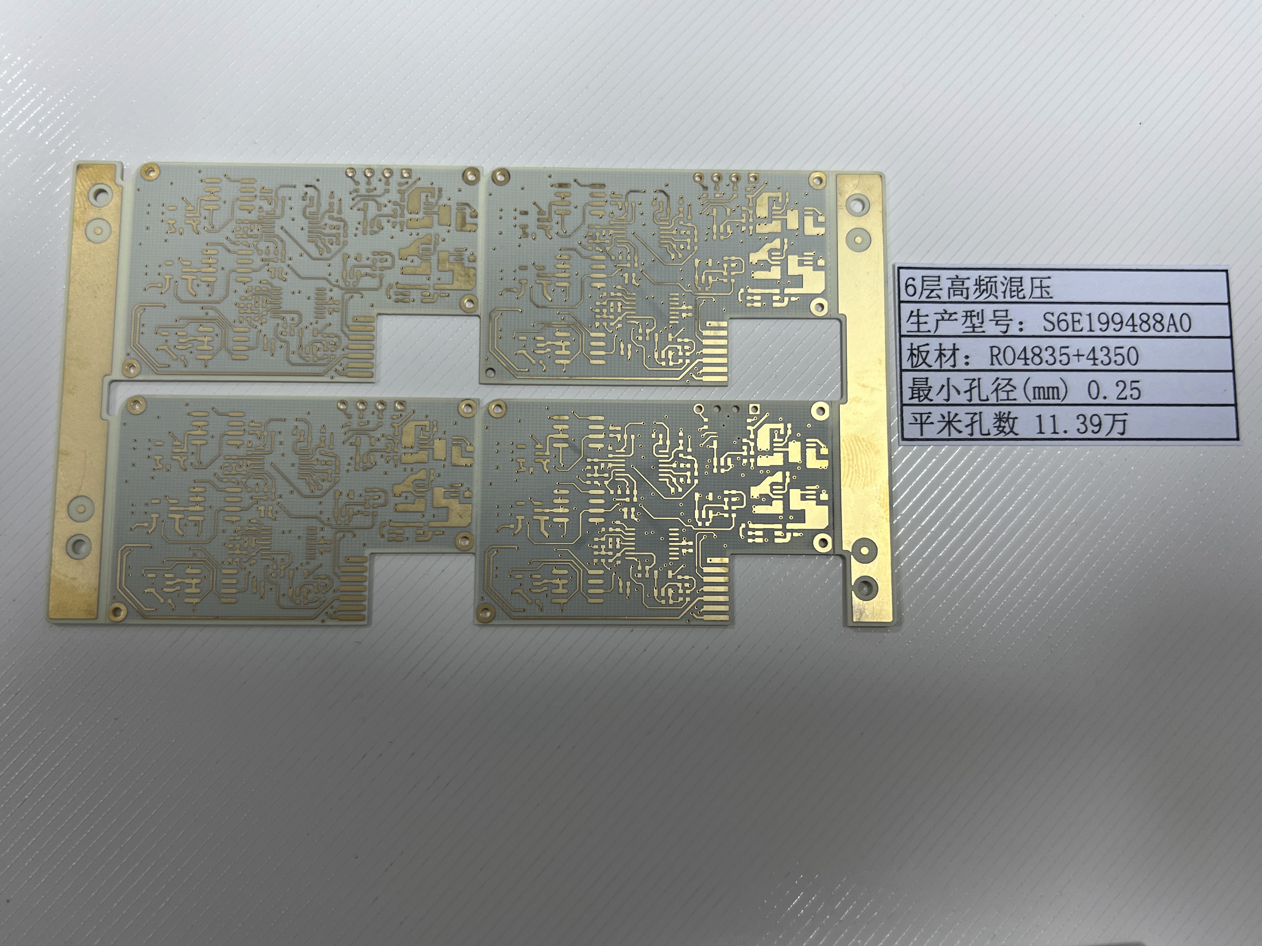
Layer Stack-Up
When you look at a multilayer pcb, you see a complex arrangement of copper and insulating layers. This structure helps you manage high-frequency rf signals. Each layer serves a specific purpose. For example, the top layer often carries rf signal traces and components. The next layer below usually acts as a ground plane, which shields signals and provides a return path. The third layer might serve as a power plane or another ground for extra isolation. The bottom layer can hold more signal traces or act as another ground.
Layer | Description |
|---|---|
Top Layer | RF signal traces and components |
Layer 2 | Ground plane for signal return paths and shielding |
Layer 3 | Power plane or additional ground for isolation |
Bottom Layer | Additional signal traces or ground |
The interaction between copper and insulating layers in a multilayer pcb is crucial. The thickness of the dielectric layer affects impedance. Thicker dielectrics raise impedance, while thinner ones can increase crosstalk. Copper thickness also matters. Thicker copper reduces signal loss but makes impedance control harder. You must balance these factors during the multilayer pcb manufacturing process to ensure signal integrity.
Vias and Connections
You use vias to connect different layers in a printed circuit board. Several types of vias exist in multilayer pcb designs:
Buried vias connect only inner layers, which helps in high-density circuits.
Microvias use lasers for drilling and support ultra-high-density routing.
Vias provide electrical pathways between layers, which is essential for complex rf circuits.
Proper via design minimizes impedance mismatches and signal distortion.
Vias also help distribute power and manage heat in the pcb.
By using vias, you can route signals in three dimensions. This approach reduces surface congestion and increases the connection density in your multilayer pcb.
Materials in RF PCBs
Choosing the right materials is key in rf pcb manufacturing. You want materials that support signal integrity, thermal management, and stable impedance. The dielectric constant of a material affects how fast signals travel and how much they lose energy. Lower dielectric constants mean faster signals and less loss.
Material Type | Properties and Applications |
|---|---|
Flexible RF PCB | Lightweight, uses polyimide substrate, copper foil, and cover-lay, good for portable devices |
Rigid Dielectrics | Low-loss, like Teflon with ceramic fillers, ideal for high-frequency systems |
Copper Foils | Surface roughness and thickness affect performance |
Polytetrafluoroethylene (PTFE) | Low dielectric constant, excellent thermal resistance, great for high-frequency applications |
Woven glass-reinforced PTFE | Superior stability, lightweight |
Ceramic-filled PTFE | Improved mechanical and thermal properties, low loss tangent |
Hydrocarbons | Cost-effective, customizable dielectric and thermal properties |
Non-PTFE materials | More affordable, easier to process, but higher risk of signal loss |
You should select materials with stable dielectric properties, especially if your printed circuit board will face temperature changes. Materials like PTFE and Rogers offer low dielectric constants and excellent electrical performance, making them popular in rf pcb manufacturing.
How Multilayer RF PCBs Work
RF Signal Transmission
You rely on a multilayer rf pcb to support high-frequency signal transmission. The design of a multilayer pcb helps you manage the challenges of radio frequency signals. When you route rf signals on the outer layers, you take advantage of the lowest effective dielectric constant. This setup allows electromagnetic waves to travel at higher speeds, especially since air further reduces the dielectric constant. You also benefit from a stable core construction. The dielectric thickness and constant remain consistent, which helps you control impedance for rf signal routing.
Dedicated ground planes in a multilayer pcb play a key role. These planes minimize interference and provide low-impedance return paths. As a result, you maintain signal integrity and reduce electromagnetic interference. In rf pcb design, you often use hybrid stack-ups with high-frequency materials. This approach enhances signal speed and quality.
Tip: Always keep rf signal traces short and direct. This practice reduces signal loss and improves overall performance.
Main Mechanisms of Signal Loss
When you work with high-frequency signals, you face several types of signal loss in a multilayer rf pcb:
Dielectric loss: As frequency increases, polarized molecules in the dielectric vibrate more, causing energy loss as heat.
Conductor loss: The resistivity of the plating material, such as copper or nickel, affects energy loss. Higher resistivity means more heat and greater loss.
Skin effect: At high frequencies, current flows mainly on the surface of the conductor. Rough or poorly conductive surfaces increase signal loss.
Copper loss: Eddy currents in copper traces force current to the outer surface, raising resistance and signal loss, especially at higher frequencies.
Design Considerations for RF
You must pay close attention to several factors in effective rf pcb design. Material selection is critical. Choose materials with a low dielectric constant (Dk) and low dissipation factor (Df) to minimize signal loss. Uniform trace width and spacing, based on impedance calculations, help you achieve controlled impedance. A proper stack-up with dedicated ground planes stabilizes signal return paths and supports signal integrity.
When you route traces, keep them short and direct. This approach avoids signal degradation. Separate high-speed and low-speed signals to prevent interference. Solid ground planes provide a continuous return path, reducing electromagnetic interference. Via stitching prevents signal leakage, and Faraday cages protect sensitive components. Avoid unnecessary vias on high-frequency traces to maintain signal strength.
Note: Impedance matching is essential in rf pcb design. If you do not match source and load impedances, you risk signal reflections and errors. Proper impedance matching improves signal integrity and power transmission.
Strategy | Description |
|---|---|
Trace Width and Separation | Adjust trace width and spacing to control impedance. |
Series and Parallel Components | Use resistors and capacitors to fine-tune impedance. |
Transmission Line Design | Implement controlled impedance lines for rf signals. |
RF Connectors and Terminations | Select connectors that match the pcb layout impedance. |
Advantages and Disadvantages
Multilayer rf pcbs offer many advantages for high-frequency applications. You gain improved signal integrity because multiple layers provide dedicated ground and power planes. This setup reduces electromagnetic interference and noise. You can design complex circuits with advanced features, such as differential pairs and precise impedance control. Flexible routing options make it easier to integrate components and save space. You can also mount surface components on both sides, which increases compactness. Miniaturization becomes possible, which is essential for modern devices like smartphones and IoT gadgets.
Advantage | Description |
|---|---|
Improved Signal Integrity | Dedicated ground and power planes reduce electromagnetic interference. |
Reduced Noise | Minimizes crosstalk and noise, boosting circuit performance. |
Complex Designs | Supports advanced features and intricate layouts. |
Flexible Routing | Offers more routing options and better space efficiency. |
Integration of Components | Allows mounting on both sides, increasing compactness. |
Miniaturization | Enables smaller, lighter devices for modern applications. |
However, you also face challenges with multilayer rf pcb manufacturing. The design process takes longer because you must plan each layer carefully. You need to consider signal integrity and thermal management. Matching the coefficient of thermal expansion (CTE) of different materials is critical to prevent issues during thermal stress. Materials for rf printed circuit boards are expensive, and any damage during fabrication can cause delays. Bonding layers requires careful surface preparation, especially with fragile materials like PTFE. If you do not manage CTE mismatches, you risk increased material waste.
Disadvantage | Description |
|---|---|
Longer Design Process | Requires meticulous planning for each layer. |
CTE Matching | Different materials must match CTE to avoid thermal stress issues. |
High Material Costs | Expensive materials increase the risk of costly delays if damaged. |
Complex Fabrication | Bonding and handling fragile materials complicate the process. |
Material Waste | CTE mismatches can lead to increased waste during fabrication. |
Applications of RF Printed Circuit Boards
You find multilayer rf pcb technology in many industries. In consumer electronics, you see these boards in smartphones, laptops, tablets, wearables, smart home devices, game consoles, and IoT gadgets. The automotive industry uses them in engine control units, ADAS components, and vehicle information systems. Industrial automation relies on rf printed circuit boards for programmable logic controllers, sensors, robotic arms, and instrumentation.
Industry | Products |
|---|---|
Consumer Electronics | Smartphones, laptops, tablets, wearables, smart home devices, game consoles, IoT gadgets |
Automotive | Engine control units, ADAS, vehicle information and entertainment systems |
Industrial Automation | PLCs, sensors, robotic arms, instrumentation |
In aerospace and defense, you use multilayer rf pcbs for military applications, atomic and nuclear systems, and aerospace computers. These boards support satellite communications and military equipment, where reliability and high-frequency performance are critical. The telecommunication industry depends on rf circuit boards for wireless communication, including Bluetooth, RFID, Wi-Fi, and cellular networks. You also see multilayer pcb designs in 5G infrastructure, where they integrate multiple signal and power layers to support antennas and transceivers. This integration ensures reliable, high-performance connectivity.
Applications of multilayer pcb extend to any field that requires high-frequency signal transmission, compact size, and robust performance. As technology advances, you will see even more applications of rf pcb in telecommunications, aerospace, defense, and consumer electronics.
You rely on a multilayer RF pcb for reliable high-frequency performance.
Multiple layers, including core and conducting layers, support signal integrity and power delivery.
Vias and careful stack-up design minimize interference.
Advantages | Disadvantages |
|---|---|
Compact, durable | Higher cost, complex |
Always weigh these factors when designing for advanced applications.
FAQ
What makes a multilayer RF PCB different from a standard PCB?
You find more layers in a multilayer RF PCB. This structure helps you manage high-frequency signals and improves performance in advanced electronic devices.
How do you choose materials for RF PCBs?
You select materials with low dielectric constants and stable properties. These materials help you maintain signal integrity and reduce energy loss.
Can you repair a multilayer RF PCB if it gets damaged?
You can repair minor surface issues. Deep internal damage often requires you to replace the entire pcb for reliable performance.
See Also
Understanding Multilayer PCBs and Their Role in Electronics
Exploring RF Circuit Boards and Their Functionality Explained
Diverse Applications of Multilayer PCBs in Various Sectors