What is an RF Circuit Board and How Does It Work
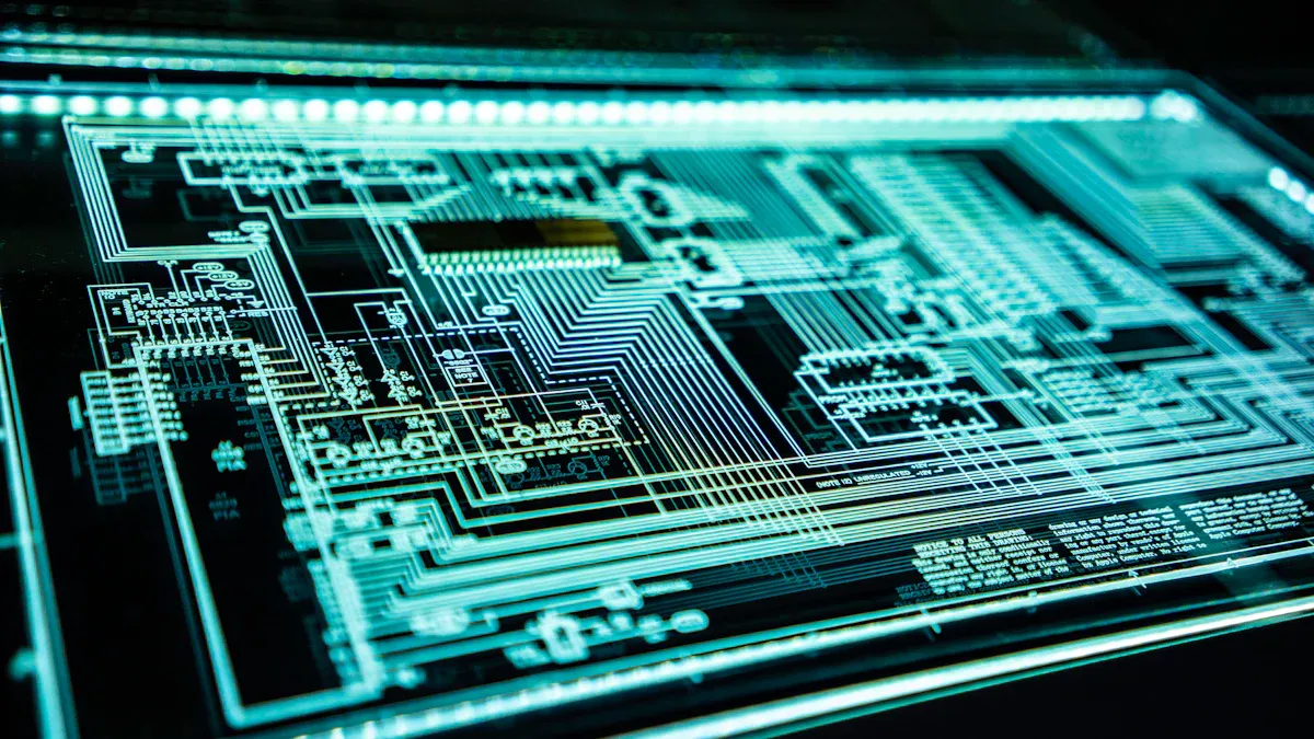
An RF circuit board is a special type of PCB made to manage radio frequency signals. These boards are important for sending and receiving high-frequency signals without losing quality. They help modern technologies like wireless systems, IoT devices, and microwave devices work smoothly.
One example shows an anticollision radar transceiver. It explains how RF circuit basics match CAD designs. This proves why accurate RF PCB design is crucial for real-world use.
The RF Evaluation Boards market shows the rising need for RF antenna PCBs and similar technologies:
Expected to grow to USD 2.9 billion by 2033.
Growing at a rate of 7.8% each year.
From microwave devices to high-frequency signals, RF circuit boards are key to improving communication and connectivity.
Key Takeaways
RF circuit boards handle fast signals, helping devices like phones work well.
Picking good materials, like PTFE and Rogers laminates, lowers signal loss and boosts performance.
Controlling impedance is key in RF PCB design to stop signal problems and make devices more reliable.
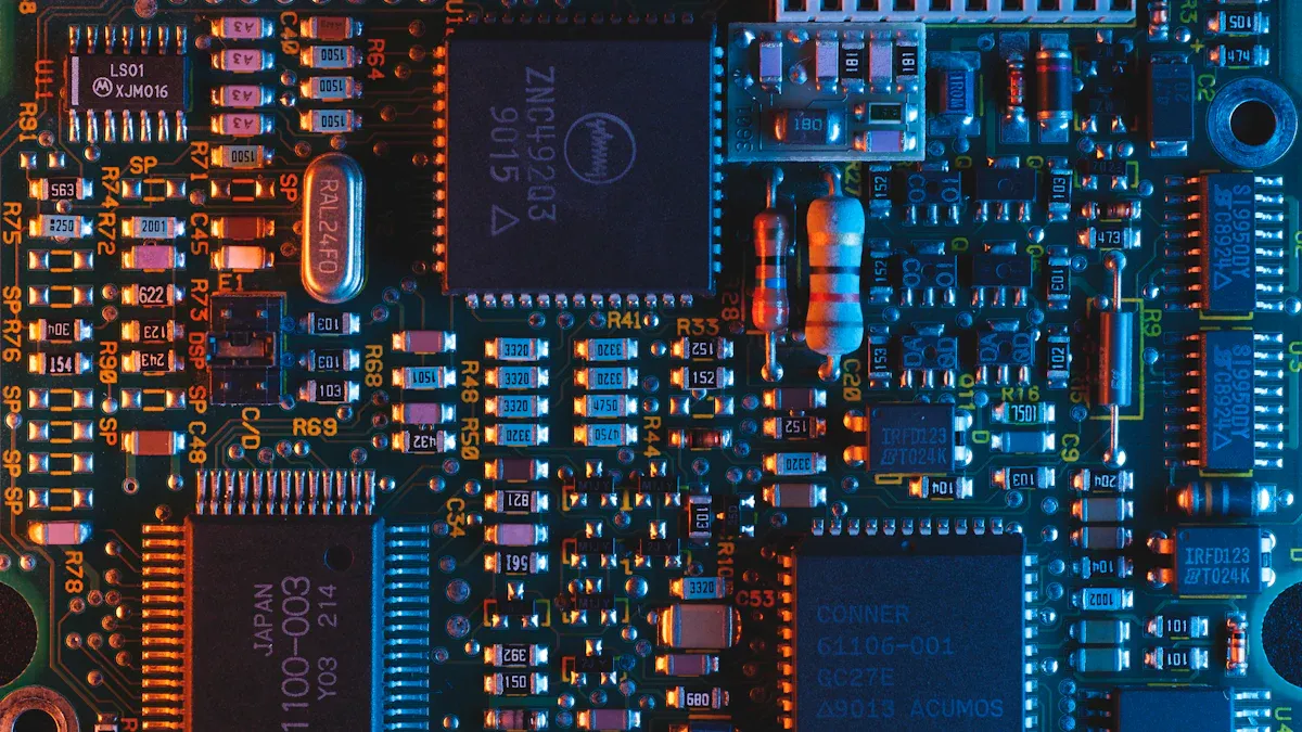
Key Features and Design Considerations of RF Circuit Boards
Materials Used in RF Printed Circuit Boards
The materials chosen for an RF circuit board are very important. They must handle high-frequency signals without problems. Common materials include PTFE, Rogers laminates, and FR-4.
PTFE: This material has great insulation and low signal loss. It keeps signals clear.
Rogers Laminates: These are good at handling heat and keeping signals stable. They work well for high frequencies.
FR-4: This is cheaper but not as good for high frequencies compared to PTFE and Rogers.
Substrate Type | Improves Signal Quality | Expands Frequency Range |
|---|---|---|
LTCC | Over 30% | Yes |
PCB | Basic | No |
Picking the right material helps your RF board work well and stay reliable.
Impedance Control in RF PCBs
Impedance control is key in RF circuit design. It ensures signals move smoothly without losing quality. Most RF PCBs use 50 Ohms impedance. This value balances power and reduces signal loss.
The 50 Ohm standard started in the early 1900s for coaxial cables.
Impedance affects how well your RF PCB handles signals.
Tools like TDR and VNA measure and adjust impedance for better performance.
Good impedance control prevents signal issues and improves your RF board's reliability.
Trace Design for Signal Integrity in RF Circuit Boards
Trace design is very important for RF circuit boards. The way traces are laid out affects signal flow. Bad trace design can cause signal loss or interference.
Shorter traces help keep signals strong and clear.
Using resistors can stop reflections and improve signal quality.
Simulation tools let you test and improve trace designs.
Design Factor | Effect on Performance |
|---|---|
Via Anti-Pad Size | Performance changes with size |
Trace Length | Longer traces reduce signal clarity |
Manufacturing Yield | Eye height: 225 DPM, Eye width: 170 DPM |
Good trace design ensures your RF board works reliably and consistently.
Rogers Materials for RF Circuit Boards Applications
Rogers materials are highly valued for RF circuit boards. They perform well in high-frequency and microwave uses.
Feature | Rogers Materials | FR4 Materials |
|---|---|---|
Dielectric Constant (Dk) | 2.5 to 11 | ~4.5 |
Thermal Conductivity | 1.0 W/mK or more | 0.1-0.5 W/mK |
Glass Transition Temperature | ~280°C | ~170°C |
Coefficient of Thermal Expansion (CTE) | Low CTE | 18 ppm |
Signal Loss | Low | Higher |
Impedance Stability | High | Lower |
These materials reduce signal loss and manage heat well. They are great for wireless devices and high-frequency tasks. Using Rogers materials makes RF boards stronger and improves signal quality.
Differences Between RF Circuit Boards and Traditional PCBs
Frequency Handling and Performance
RF circuit boards are great for high-frequency signals. They use special materials like PTFE and Rogers laminates. These materials have low dielectric constants and reduce signal loss. This helps signals travel better and faster. Traditional PCBs use FR-4, which is not as good for high frequencies.
The table below shows how RF and traditional PCBs differ:
Attribute | RF Circuit Boards | Traditional PCBs |
|---|---|---|
Material Selection | Special materials like PTFE, RO4003 | Standard materials like FR-4 |
Layer Stacking | Many layers for better impedance control | Fewer layers, less focus on impedance |
Impedance Control | Tight control for specific values | Looser control, less important |
Trace Width and Spacing | Carefully designed for high frequencies | Standard design |
Via Placement | Strategically placed for signal quality | General placement |
Grounding | Low-impedance paths for better performance | Basic grounding |
Shielding | Often includes shielding | Rarely includes shielding |
These features make RF PCBs perfect for 5G and other high-frequency uses.
Design Challenges in RF PCBs
Designing RF PCBs is tricky and needs careful planning. You must manage impedance, trace layout, and materials. Small mistakes can cause big problems like signal loss or interference.
Common design problems include:
Floating copper or solder mask slivers that create noise.
Starved thermals causing soldering and function issues.
Small annular rings leading to open circuits.
Copper too close to edges, causing shorts.
Testing helps solve these problems. For example:
Testing Type | Purpose |
|---|---|
Thermal Cycling | Checks if PCBs handle quick temperature changes. |
Vibration Testing | Ensures PCBs survive physical stress during use. |
Vacuum Exposure | Tests if PCBs work in a vacuum without damage. |
By fixing these issues, RF PCBs can work well in tough conditions.
Advantages of RF Printed Circuit Boards
RF PCBs have many benefits over regular PCBs. They prevent signal loss, reduce interference, and control impedance better. These features keep signals strong, even at high frequencies.
Key benefits include:
Special materials that reduce signal loss and improve efficiency.
Precise impedance control to avoid signal problems.
Advanced grounding and shielding to lower interference.
Compact designs for small devices and tight spaces.
The table below highlights these advantages:
Benchmark | Description |
|---|---|
Signal Integrity | Keeps signals clear and reliable in high-frequency systems. |
Impedance Matching | Ensures components work together without signal reflection. |
Noise Reduction | Uses grounding and shielding to reduce interference. |
Low Losses | Uses materials that keep signals strong and efficient. |
Heat Dissipation | Designed to handle heat and prevent damage. |
Miniaturization | Allows small designs for portable devices. |
Frequency Performance | Works well across a wide range of frequencies. |
These features make RF PCBs essential for 5G, IoT, and advanced communication systems. They handle high frequencies with precision, making them key to modern technology.
Applications of RF Circuit Boards in Modern Industries
Wireless Communication and RF PCBs
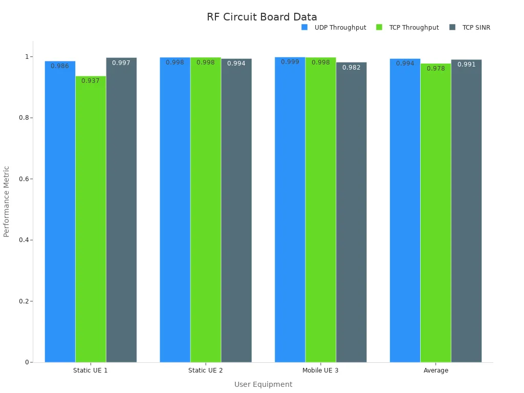
RF PCBs are crucial for wireless communication. They help send signals reliably in devices like phones, routers, and smartwatches. These boards handle fast signals, making them perfect for 5G and advanced tech. The need for smaller, better wireless devices has improved RF PCB designs.
Performance data shows their efficiency. For instance, RF PCBs reach TCP throughput of 0.978 and UDP throughput of 0.994. This ensures fast data transfer. Scientists use tools like Colosseum to test RF PCBs in real-world setups. These tests prove their reliability in wireless systems.
Radar and Satellite Systems Using RF Circuit Boards
Radar and satellites depend on RF PCBs for high-frequency tasks. Modern radar systems use AESAs with flat 2D designs. These designs make them more reliable and easier to build. Satellites in Ka and V bands use RF PCBs for faster communication with more bandwidth.
Important improvements include:
Better AESA designs for stronger performance.
Higher frequency bands for quicker data transfer.
These features make RF PCBs vital for radar and satellite systems. They ensure accurate and efficient operations.
IoT and Smart Devices with RF Printed Circuit Boards
IoT gadgets rely on RF PCBs for smooth connections. These boards support smart home devices, factory sensors, and wearables. The IoT RF PCB market is growing fast, expected to hit USD 69 billion by 2032.
Reasons for this growth include:
More RF PCBs used for fast data sharing.
Need for low-power, high-speed connectors.
Advances in 5G and IoT technologies.
RF PCBs make sure data moves smoothly, which is key for IoT devices. They help wireless communication grow in many industries.
RF circuit boards are crucial for handling high-frequency signals accurately. They help wireless communication, IoT, and healthcare systems work well. Choosing the right materials and controlling impedance make them more effective.
The RF PCB market is growing fast due to 5G and IoT progress.
Proof of RF PCB Improvements
Proof Type | Details |
|---|---|
Data | RF sensing tech offers affordable ways to monitor people and environments. |
Real-Life Examples | Studies show RF tech works well for health monitoring and smart sensing. |
Performance Results | RF sensing accurately tracks breathing and heartbeats, proving its use in healthcare. |
The RF PCB market is growing 7.5% yearly from 2023 to 2030.
It was worth USD 8.5 billion in 2022 and may reach USD 12.2 billion by 2028.
5G and IoT devices are the main reasons for this growth.
RF circuit boards are key to improving wireless communication and IoT. They ensure smooth connections and drive innovation in many fields.
FAQ
What does an RF circuit board do?
An RF circuit board handles high-frequency signals. It keeps signals clear for wireless devices, IoT, and radar systems.
How are RF circuit boards different from regular PCBs?
RF circuit boards use special materials and careful designs. These help them work better with high-frequency signals than regular PCBs.
Why is impedance control needed in RF circuit boards?
Impedance control helps signals move smoothly. It reduces signal loss and interference, which is important for high-frequency uses.
See Also
Exploring Rogers R4350B, R4003, And R5880 For RFPCB Use
Defining PCB Printed Circuit Boards And Their Key Principles
The Role Of Multilayer PCBs In Modern Electronic Devices
Unveiling Cutting-Edge HDI PCB Prototyping Methods Now
Maximizing Budget Efficiency With Quick Turn HDI PCBs In 2025