What is a Copper Clad PCB Board and How Does It Work
A copper clad PCB board gives you a solid foundation for building electronic circuits.
Copper traces create pathways for electrical connections between parts.
These traces guide signals and help reduce wiring complexity and space.
Region/Industry | Growth Rate (CAGR) | Key Drivers | |
|---|---|---|---|
U.S. | 75.4% | 4.8% | Advanced electronics manufacturing, high-tech industries |
Germany | N/A | N/A | Strong industrial base, automotive and industrial automation sectors |
China | 30.7% | 5.5% | Expansive electronics manufacturing sector, global production hub |
Key Takeaways
Copper clad PCB boards serve as the foundation for electronic devices, providing pathways for electrical connections.
Choosing the right copper thickness is crucial for performance; thicker copper improves current handling and reduces signal loss.
Copper clad laminates are versatile and used in various applications, from consumer electronics to aerospace, ensuring reliable performance.
Copper Clad PCB Board Basics
What is a Copper Clad PCB Board?
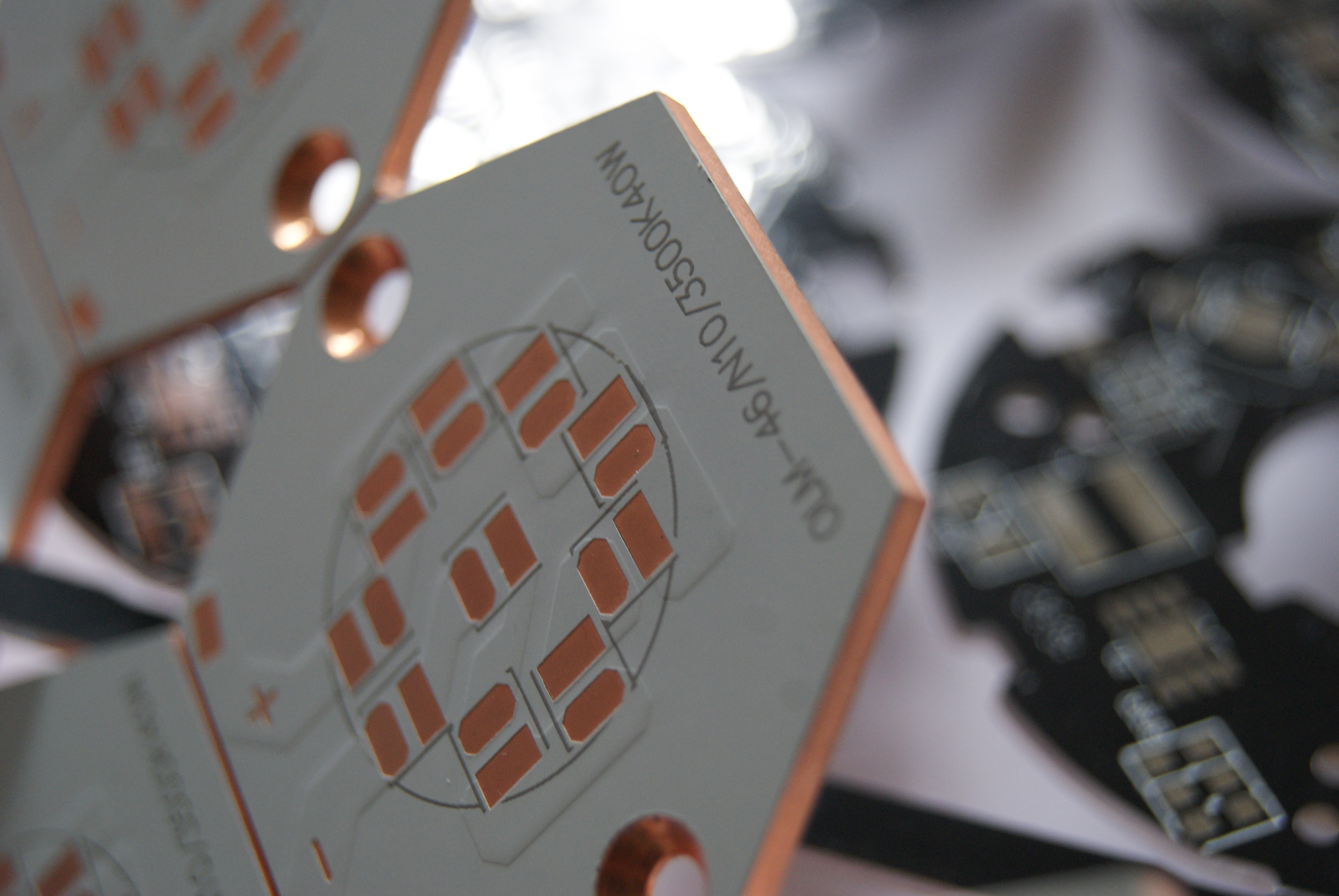
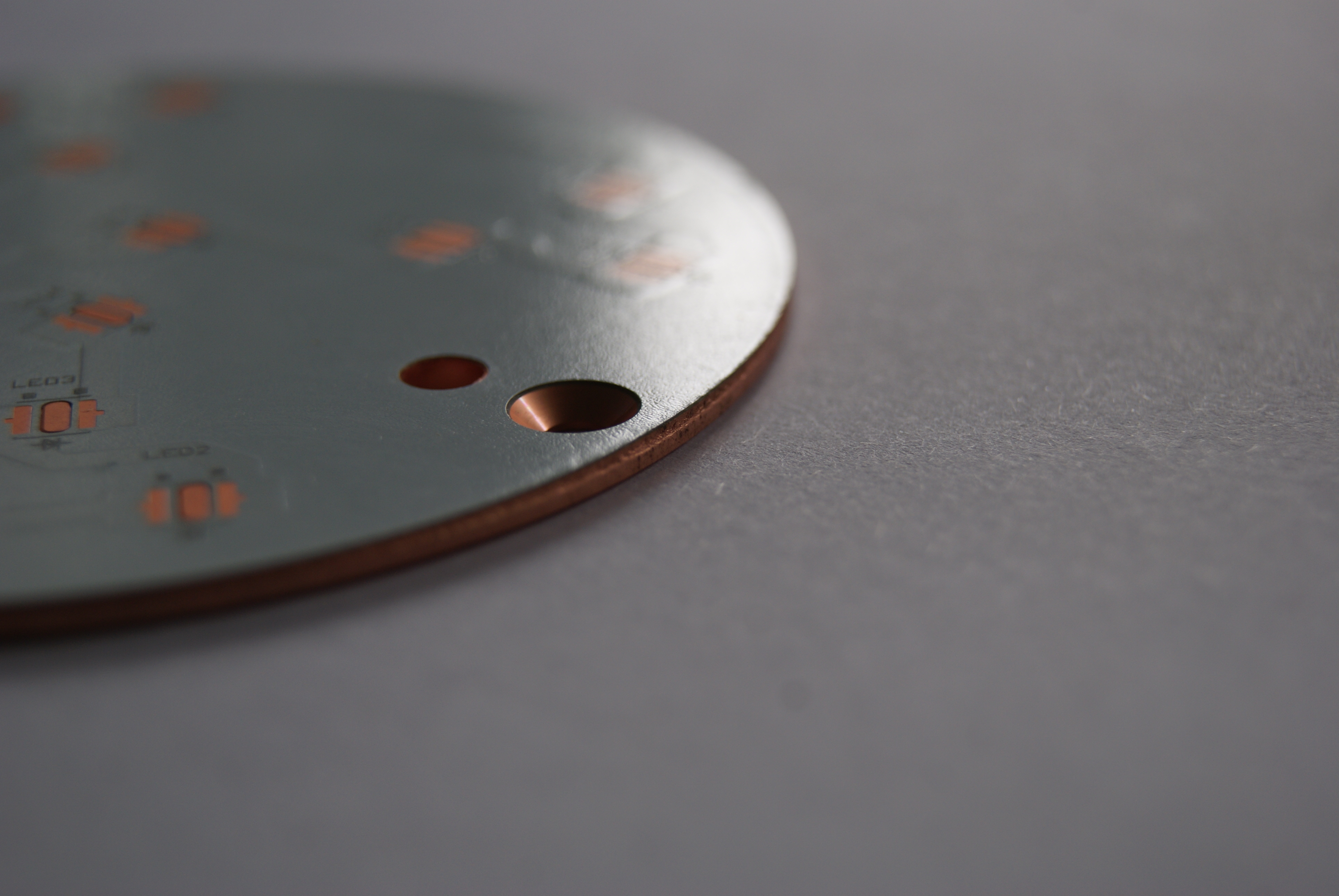
You use a copper clad PCB board as the foundation for most electronic devices. This board starts with a base material, such as fiberglass or resin, and gets covered with a thin layer of copper on one or both sides. The copper layer allows you to create pathways for electricity, which connect different parts of your circuit.
It is laminated with a thin layer of copper on one or both sides.
You find copper pcb boards in almost every electronic product, from smartphones to industrial machines. The copper layer provides excellent electrical conductivity, which is essential for reliable circuit operation. When you design a pcb, you choose the right copper clad laminate to match your application's needs. LT CIRCUIT uses advanced copper clad laminates to ensure high performance and reliability in all their products.
Copper PCB Board Structure
A copper pcb board contains several layers, each with a specific function. Understanding these layers helps you see how the board supports complex circuits and applications.
Layer Type | Description |
|---|---|
Signal Layer | Connects components and affects performance and reliability. |
Power Layer | Connects the power supply and ground wire for stable power. |
Ground Layer | Connects ground wires for stable ground connections. |
Pad Layer | Connects components to the pcb board. |
Assembly Layer | Arranges installation positions and methods for component assembly. |
Solder Mask Layer | Prevents short circuits and protects the pcb during soldering. |
Copper Layer | Provides circuit connections and supports signal transmission lines. |
The copper layer forms the main pathways for your circuit. The solder mask layer protects these pathways during pcb fabrication and assembly. The pad layer allows you to attach components securely. When you use a double sided copper pcb board, you get copper layers on both sides, which increases the complexity and capability of your circuit boards.
The thickness of the copper layer plays a big role in how your copper pcb board performs:
Enhanced thermal management: More copper helps spread heat, keeping your components safe.
Reduced voltage drop: Thicker copper keeps voltage steady across the circuit.
Better signal integrity: Thicker copper reduces signal loss, which is important for high-speed or RF applications.
Mechanical durability: More copper makes the board stronger and more resistant to damage.
Industry standards like IPC-2221 and IPC-2152 guide you in choosing the right copper thickness for your pcb design.
LT CIRCUIT uses Panasonic’s high-performance copper clad laminates, which offer tight control over dielectric properties and thermal stability. These features make LT CIRCUIT’s copper pcb boards ideal for demanding applications, such as 5G networks and automotive electronics.
Materials Used in Copper Clad Boards
You can choose from several materials when selecting a copper clad pcb board. The base material, or substrate, affects the board’s strength, flexibility, and performance.
Metal base copper clad laminate
Epoxy glass fiber cloth substrate
Paper substrate (phenolic and epoxy)
Polyimide (PI) flexible copper clad laminate
Special resin glass fiber cloth substrate
FR4 is the most common material for copper pcb boards. It offers a balance of strength, cost, and performance. Here are some key properties of FR4:
Property | Description |
|---|---|
Strength | FR4 is tough and steady, providing good support and flexibility. |
Cost-Effectiveness | It is affordable, costing about $5 to $15 per square meter. |
Flame Resistance | The material resists combustion and slows down the spread of flames. |
Durability | It withstands mechanical stress and resists moisture and humidity. |
Electrical Properties | High dielectric strength and low dissipation factor make it an excellent insulator. |
Thermal Resistance | Good thermal resistance allows performance in high-temperature applications. |
You also find copper clad laminates made from special resins or flexible materials for unique applications. LT CIRCUIT selects the best copper clad laminate for each project, ensuring that your printed circuit boards meet the highest standards for electrical conductivity, durability, and reliability.
When you work with LT CIRCUIT, you benefit from their focus on quality and innovation. They use copper clad laminates with consistent dielectric properties and low signal loss, which is important for advanced applications of copper clad laminates in modern electronics. Their expertise in pcb fabrication ensures that your copper pcb board will perform well in any application, from single sided copper clad board designs to complex multilayer circuit boards.
Applications and Types of Copper Clad Boards
Applications of Copper Clad Laminates
You encounter copper clad laminates in almost every area of electronics. These materials form the backbone of modern circuit boards and support a wide range of applications. Here are the most common uses:
Consumer electronics: You find copper clad PCB boards in smartphones, tablets, and laptops. These devices rely on the conductive surface and mechanical support provided by copper clad laminates.
Industrial equipment: Copper clad boards help control and monitor processes in factories and machinery.
Aerospace and defense: Avionics and radar systems depend on the reliability and performance of copper clad laminates.
Telecommunications: Routers, base stations, and network equipment use copper clad PCB boards for signal transmission and stability.
Copper clad laminates support the miniaturization and enhanced functionality of electronic components. The growing demand for compact and high-performance devices drives the expansion of the copper clad laminate market.
Contribution | Description |
|---|---|
Conductive Surface | The copper layer acts as the conductive surface for circuit traces, essential for signal transmission. |
Mechanical Support | The substrate provides mechanical support for the electronic components attached to the PCB. |
Foundation for Circuitry | Copper clad laminates enable the creation of intricate circuitry in electronic manufacturing. |
Copper clad PCB boards also contribute to energy efficiency. Low electrical resistance in copper clad laminates improves current flow, which reduces power consumption in devices like smartphones and electric cars.
Types of Copper Clad PCB Boards
You can choose from several types of copper clad PCB boards depending on your application. Each type offers unique advantages for different circuit designs.
PCB Type | Applications | Advantages | Disadvantages |
|---|---|---|---|
Used in simple devices like calculators, LED lighting, and printers. | Simplicity and low cost. | Limited space for complex circuits. | |
Double-Sided | Common in complex devices like cellphones, amplifiers, and automotive systems. | More area for conductors, suitable for compact designs. | Higher fabrication costs. |
Single sided copper clad board: Ideal for camera systems, radio equipment, power supplies, and timing circuits.
Double sided copper pcb board: Used in vending machines, cellphones, UPS systems, amplifiers, and car dashboards.
You also find copper clad laminate circuit boards in specialized forms:
Copper strip PCB board: Handles high-current circuits.
Copper clad plate laminate PCB board: Known for high strength.
Ceramic or metal-core boards: Used for high-frequency applications.
LT CIRCUIT offers a wide range of options, including HDI and multilayer boards. You can select the number of layers, surface finish, and solder mask color to match your pcb design needs. Their advanced pcb fabrication process ensures high quality and reliability for every project.
Benefits and Limitations
Copper clad PCB boards deliver several key benefits for your circuit boards:
Benefit | Description |
|---|---|
Promotes efficient transmission of electrical signals, reducing risk of signal loss or distortion. | |
Exceptional Thermal Conductivity | Effectively dissipates heat, reducing chances of thermal issues in PCBs. |
Exceptional Durability | Improves resilience and resistance to bending or fracturing, crucial for high-stress environments. |
Exceptional Chemical Resistance | Withstands exposure to chemicals, ensuring longevity and maintaining electrical performance. |
Versatility in Manufacturing | Easily integrated into various processes, enabling cost-effective production of complex designs. |
Exceptional Dimensional Stability | Maintains shape and dimensions under varying conditions, ensuring structural integrity. |
Accessibility in the Market | Readily available, ensuring consistent supply and cost-effectiveness for manufacturers. |
You benefit from the versatility and reliability of copper clad laminates in high-frequency circuits. These boards maintain signal integrity and resist thermal and chemical stress.
However, you should consider some limitations when selecting copper clad boards for industrial use:
Copper clad laminate is more expensive than alternatives like aluminum substrates.
Large thermal expansion coefficient can lead to bending or cracking under temperature changes.
Strong acids, alkalis, or high temperatures may damage the copper clad PCB board.
Proper grounding and spacing in your circuit layout help prevent noise issues, especially in high-frequency applications.
Selection Tips for PCB Boards
When you choose a copper clad PCB board for your project, you need to evaluate several factors. The right selection ensures your circuit boards meet performance, cost, and reliability requirements.
Factor | Details |
|---|---|
Substrate type and copper thickness impact cost and performance. | |
Layer Count & Stack-Up | More layers increase costs significantly due to additional materials and processes. |
Order Volume | Larger orders reduce per-unit costs due to economies of scale. |
Surface Finish & Coating | Premium finishes and coatings add to the overall cost. |
Tolerance & Specification | Tight tolerances and controlled impedance requirements increase costs. |
Lead Time & Urgency Fees | Rush orders and expedited shipping can significantly raise expenses. |
Certification & Compliance | Meeting industry standards and regulations can add to costs. |
Secondary Operations | Additional features and assembly services increase overall project costs. |
LT CIRCUIT helps you customize your copper clad PCB board to fit your exact needs. You can specify the layer count, choose from different surface finishes, select solder mask colors, and request tailored testing services. Their commitment to quality and innovation ensures your pcb fabrication meets the highest standards.
Customization Aspect | Description |
|---|---|
Layer Count | You can specify the number of layers needed for your pcb design. |
Surface Finish | Choose from different surface finishes to suit your application requirements. |
Solder Mask Color | Select custom colors for solder masks to meet aesthetic or functional needs. |
Testing Services | Request tailored testing services to ensure the pcb meets specific performance criteria. |
You should also consider certifications and standards for critical applications. For example, IPC-6012 Class III and UL Certification ensure safety and reliability in aerospace, medical, automotive, and industrial circuit boards.
LT CIRCUIT stands out for its advanced materials, strict quality control, and strong customization options. You receive excellent support and clear communication throughout your project. Their reliability and innovation make them a top choice for copper clad PCB boards in any application.
Copper clad PCB boards give you reliable performance and support next-generation electronics. LT CIRCUIT uses advanced materials and innovative processes to meet your needs. You benefit from high-quality solutions, even as trends like 5G and electric vehicles shape the future. The cost of the pcb remains competitive as technology advances.
Impact on Copper Clad PCB Boards
Advancements in materials
Enhances performance and durability of PCBs
Increased demand for high-frequency applications
Drives innovation in laminate technology
Focus on sustainability
Promotes eco-friendly materials
Proliferation of consumer electronics
Expands market opportunities for CCLs
Rollout of 5G technology
Necessitates high-performance laminates
Adoption of electric vehicles
Increases demand for advanced CCLs
FAQ
What is the main purpose of a copper clad board?
You use a copper clad board to create electrical connections and support components in electronic devices. It forms the base for your pcb design.
How do you choose the right copper thickness?
You select copper thickness based on current requirements, heat management, and signal integrity. Thicker copper handles more current and improves durability.
Can you use copper clad boards for flexible circuits?
You can use flexible copper clad laminates for circuits that need to bend or fold. These boards work well in wearable devices and compact electronics.
See Also
Utilizing Panasonic Copper-Clad Laminates for PCB Production
Understanding PCB Printed Circuit Boards and Their Fundamentals
Guide to Manufacturing Heavy Copper Multilayer PCBs
Components That Constitute Printed Circuit Boards Explained
Using Horizontal Copper Sinking Technology in PCB Manufacturing