What is an HDI Flex PCB and How Does It Work
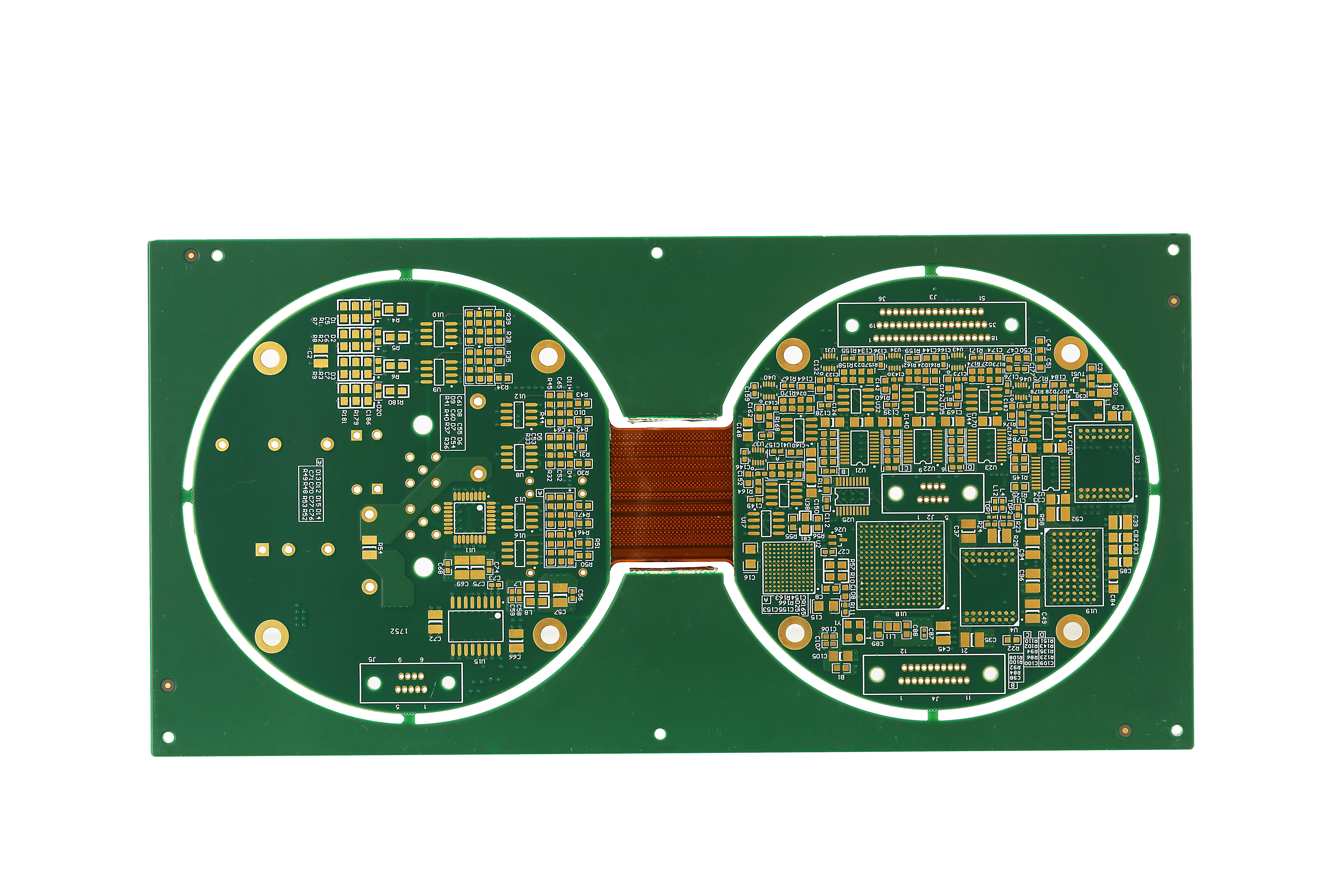
An hdi flex pcb combines high-density interconnect technology with flexible materials, allowing for advanced, compact, and multi-layer circuit designs. By utilizing microvias, an hdi flex pcb can achieve greater circuit density in a smaller footprint compared to standard flex circuits. These hdi flex pcb solutions maintain strong signal integrity and deliver reliable long-term performance. As the demand for flexible circuits continues to grow due to their versatility, LT CIRCUIT is dedicated to enhancing the performance and durability of hdi flex pcb products, ensuring they meet the evolving needs of modern electronics.
Key Takeaways
HDI flex PCBs have small microvias and bendy materials. They can fit more circuits in a tiny, flexible space. This helps make devices smaller and smarter.
These PCBs keep signals strong and clear with special designs. The designs lower noise and help fast communication.
HDI flex PCBs are strong and dependable. People use them in cars, medical tools, and electronics. They help make gadgets light and flexible.
HDI Flex PCB Overview
What Is an HDI Flex PCB
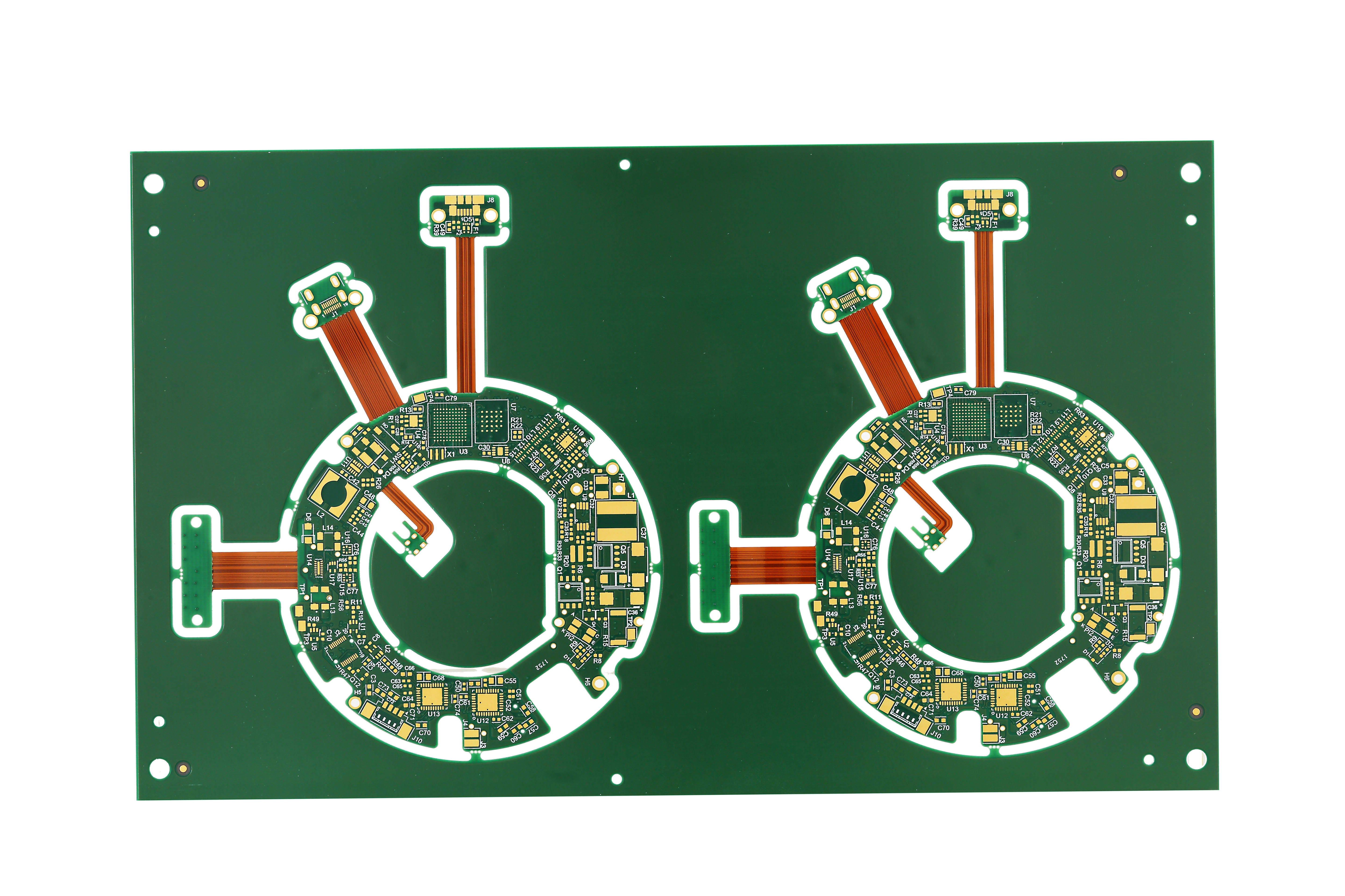
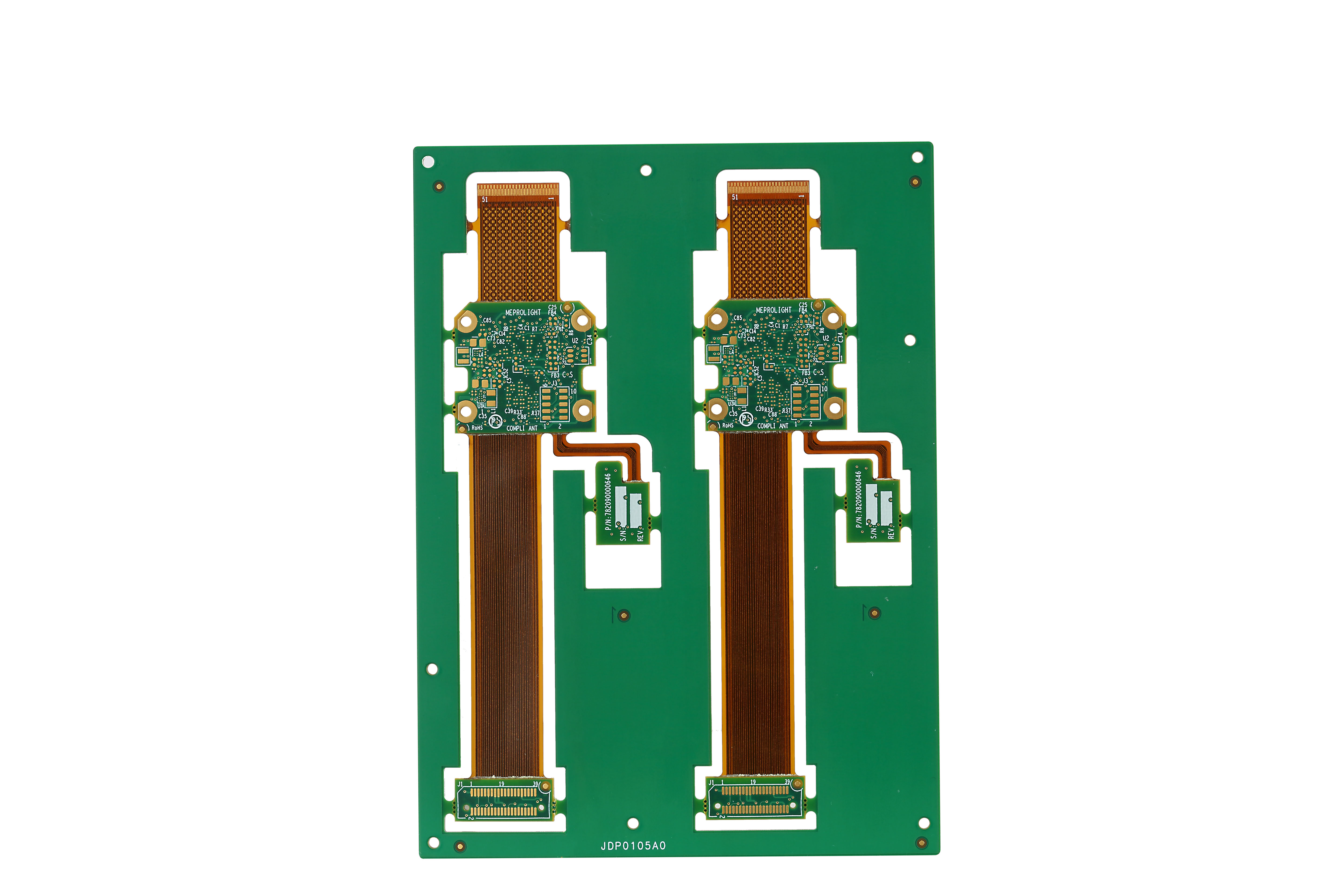
An hdi flex pcb is a flexible printed circuit board. It uses high-density interconnect technology. This lets engineers fit more circuits in a small space. High density interconnect flex circuits have micro-via structures. These are tiny holes that link the layers of the pcb. Some micro-via features are only 50 micrometers wide. Thin materials like polyimide make these circuits light and bendy. This mix of flexibility and high circuit density makes hdi flex pcb different from regular flex circuits and rigid printed circuit boards.
The table below lists the main technical features of an hdi flex pcb:
Characteristic | Description / Specification |
|---|---|
Microvia size | Minimum 75 μm, 50 μm finished |
Line width and spacing | Down to 50 μm |
Dielectric thickness | As low as 25 μm |
Copper thickness | Starting from 9 μm |
Via types | Blind and buried vias using sequential build technology |
Materials | Polyimide films (various thicknesses), copper conductors |
Surface finishes | OSP, Immersion Silver, Immersion Tin, ENIG, ENEPIG, etc. |
Mechanical features | Fold lines, thinned bending zones, cut-outs |
Component packaging | Supports chip-on-flex (COF), BGAs, chip scale packaging |
Electrical & thermal benefits | Improved signal integrity, thermal performance, reliability |
Layer count | 3 to 16 layers |
High-density interconnect flex circuits use these features for high signal density. They also support high-density parts. LT CIRCUIT is a top provider of advanced hdi flex pcb solutions. Their products meet strict quality and performance rules.
How HDI Flex PCBs Work
HDI flex pcb technology uses micro-via, blind via, and buried via. These are used instead of regular through-hole vias. Micro-via connections help make the circuits smaller and more complex. Fine traces and small vias help signals stay strong and move fast. High-density interconnect flex circuits use impedance-controlled routing. This keeps signal quality high, which is important for devices that need good communication.
Micro-via technology makes signal paths shorter and lowers noise. This helps keep signals clear in fast circuits.
The main idea of hdi flex pcb is stacking thin layers. Each layer connects with micro-via. This design lets the board hold more parts and wires without getting bigger. Special steps like laser drilling and sequential lamination are used. These steps make sure micro-via are placed right and layers stick together well. These features make hdi flex pcb great for new devices that need to be small and work well.
Key Features and Structure
An hdi flex pcb has many thin dielectric layers, flexible substrates, and micro-via connections. Polyimide or liquid crystal polymer substrates give flexibility and strength. Micro-via, blind via, and buried via allow dense routing and high signal density. Advanced lamination bonds the layers, making the board strong and reliable.
Key features of hdi flex pcb are:
More parts can fit because of micro-via and small pads
Flexible sections let the board bend and twist
Space is saved by mixing rigid and flexible parts
Better reliability comes from less stress and strong materials
Designs can be more complex and even 3D
Signal integrity and controlled impedance are very important
The chart below shows how many pcbs of each type were made in 2024:
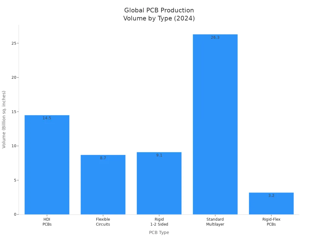
HDI flex pcb solutions make up a big part of the world market. They are made more than flexible circuits. Flex circuits are still needed for many uses. But high-density interconnect flex circuits give higher circuit density, better signal integrity, and support for fast signals. LT CIRCUIT leads the way by making strong, high-performance hdi flex pcb products for many devices.
Manufacturing and Benefits
Manufacturing Process
Manufacturers make HDI flex circuits using careful steps. They start by picking materials like polyimide and copper foil. The substrate is prepared with copper foil. Then, photoresist is put on the surface. UV light helps transfer the circuit pattern. Unwanted copper is removed by etching. Layers are built up one at a time. This is called sequential lamination. Laser drilling makes microvias to connect layers. Copper plating fills the microvias and covers the board. The outer layers get a solder mask and finishes like ENIG. Each board goes through many tests. These include Automated Optical Inspection and X-ray checks. LT CIRCUIT uses special tools and follows strict rules like ISO 9001 and IPC. This makes sure every pcb is strong and works well.
Advantages of HDI Flex PCBs
HDI flex circuits have many good points. They help make devices smaller and lighter. Microvias and thin traces let more circuits fit in less space. Shorter signal paths help signals stay strong and clear. These circuits are also tough and last a long time. They work well in places with lots of movement or shaking. Polyimide layers protect the circuits better than old solder masks. Using fewer connectors and cables means fewer things can break. This makes flex circuits great for high-performance jobs.
Applications of Flexible Circuits
Flexible circuits are used in many fields. The table below lists some common uses:
Industry | |
|---|---|
Automotive | LED strips, sensors, infotainment, airbags, interior electronics |
Medical | Wearable monitors, drug delivery, ultrasound, diagnostic equipment, remote health monitoring |
Consumer Electronics | Smartphones, wearables, speakers, earphones, portable displays, touch controls, LED strips |
Flex circuits let designers add more features to small devices. Their bendy shape and high circuit density are important for new electronics.
Design Considerations
Designers face some problems with HDI flex circuits. Making small boards with good part layout takes planning. Signal problems like crosstalk and impedance mismatch can hurt how they work. Smooth changes between flex and stiff parts stop stress. Good heat control is needed in tight layouts. LT CIRCUIT uses smart CAD tools and automatic systems to help. They also use strong quality checks. Their skills make sure each flex circuit is reliable and meets high standards.
Tip: Work early with skilled makers like LT CIRCUIT. This helps make flexible circuits that work well and are easy to build.
HDI flex pcb technology is changing electronics for the better.
Flex pcb designs help make smaller and faster devices.
Flex pcb is used in medical, car, and home gadgets.
Flex pcb helps signals stay clear and power work well.
In the future, hdi flexible pcb will use new materials and smart designs.
Flex pcb will stay important as people want better and smaller pcb products.
Flex pcb is tough and works well in hard places.
Flex pcb is good for IoT, AI, and 5G devices.
Flex pcb keeps making every pcb market move forward.
FAQ
What makes a flex pcb different from a regular pcb?
A flex pcb bends and twists, while a regular pcb stays rigid. Flex circuits use special materials. These materials allow the pcb to fit into tight spaces.
Can a flex pcb handle high-speed signals?
Yes, a flex pcb supports high-speed signals. Engineers design the pcb with controlled impedance. This keeps the signals clear and stable in the flex circuit.
Why do designers choose a flex pcb for new devices?
Designers pick a flex pcb because it saves space. The pcb can fold or curve. This lets the flex circuit fit inside small or oddly shaped devices.
Tip: A flex pcb also reduces the number of connectors. This makes the pcb more reliable and easier to assemble in complex electronics.
See Also
Compact And Durable HDI Rigid Flex Circuit Boards
The Process Behind Designing And Making HDI Multi-Layer PCBs
Understanding The Laser Hole Via Filling Technique In HDI PCBs
Advantages Of LDI Exposure Machines For HDI PCB Circuit Production