What Is an HDI PCB and How Does It Work
HDI PCB, or high-density interconnect printed circuit board, enables compact, high-performance devices. The HDI market is expanding rapidly, driven by demand for miniaturized electronics in sectors like 5G and automotive. LT CIRCUIT leads in HDI PCB manufacturing, delivering advanced circuit board solutions for today’s evolving technology.
Key Takeaways
HDI PCBs use tiny microvias and build-up layers to fit more connections in a smaller space, making devices smaller and faster.
Compared to traditional PCBs, HDI PCBs offer better signal quality, support more complex designs, and work well for advanced electronics like 5G and automotive systems.
Industries like mobile devices, aerospace, medical, and automotive rely on HDI PCBs for reliable, high-performance products that save space and improve functionality.
HDI PCB Basics
What Is HDI PCB
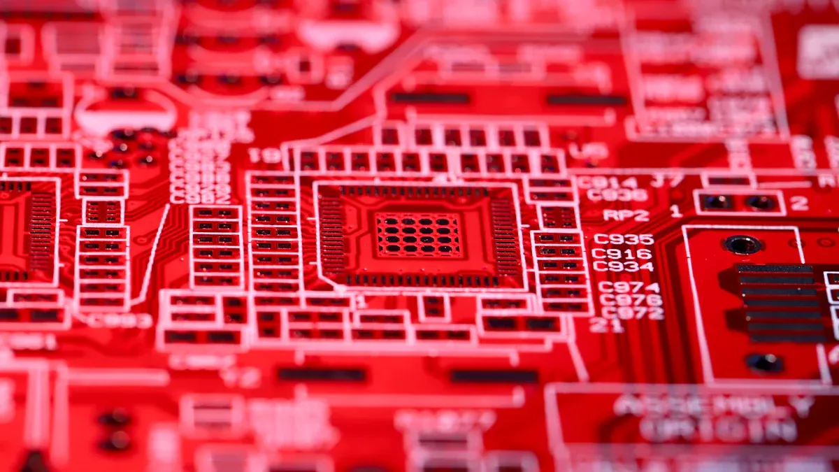
HDI PCB stands for high-density interconnect printed circuit board. This type of PCB uses advanced technologies to achieve higher wiring density and compact layouts. Engineers use microvias, blind vias, and buried vias to connect different layers in the PCB stackup. Microvias, created by laser drilling, often have diameters less than 150 micrometers. These small vias allow for denser routing and more components in a smaller area.
HDI PCBs often feature multilayer stackups such as 2+N+2 or Every Layer Interconnect (ELIC). These configurations support complex circuits and high-layer count designs. The aspect ratio of microvias is typically 0.75:1, which improves plating and thermal performance. Drill-to-copper clearance values usually range from 7 to 8 mils, ensuring precise manufacturing.
HDI PCBs enable advanced pcb design by supporting fine line widths and tight spacing between components. This results in compact, high-performance devices that meet the demands of modern electronics.
Key features of HDI PCBs include:
Microvias with diameters under 150 micrometers for denser routing.
Layer counts ranging from 4 to over 10, increasing wiring density.
Build-up layers that allow for flexible stack-up options.
Improved signal integrity due to shorter signal paths.
HDI vs. Traditional PCB
HDI PCBs differ from traditional PCBs in several important ways. The table below highlights the main differences:
Comparison Factor | HDI PCBs | Traditional PCBs |
|---|---|---|
Layer Count | Supports significantly more layers (up to 16 or more) | Typically limited to 6 or fewer layers |
Via Design | Uses smaller blind, buried, and microvias enabling higher density | Mostly uses larger through-hole vias |
Signal Integrity | Superior signal integrity due to shorter signal paths and controlled impedance | Lower signal integrity with longer signal paths |
Functionality | Higher functionality supporting advanced components like BGAs | Lower functionality with simpler component support |
Complexity and Cost | More complex and costly manufacturing involving laser drilling and precise control | Simpler and less expensive to produce |
HDI PCBs use thin cores and build-up layers to achieve high interconnect density. Laser-drilled microvias provide precise 3D connections between layers, which improves electrical performance. Traditional PCBs rely on thicker cores and larger vias, which limits their density and functionality. HDI PCBs support high-speed and high-frequency signals, making them ideal for advanced applications.
LT CIRCUIT HDI PCB Features
LT CIRCUIT stands out as a leader in HDI PCB manufacturing. The company uses state-of-the-art microvia technology and advanced materials to deliver reliable, high-performance PCBs. LT CIRCUIT offers a wide range of stack-up options, including multilayer and any-layer HDI PCBs. Their products feature high interconnect density, fine line widths, and precise pcb layout.
LT CIRCUIT’s HDI PCBs include:
Multiple build-up layers for flexible stack-up configurations.
Microvias, blind vias, and buried vias for enhanced routing and connectivity.
High density and compact pcb design for modern electronic devices.
Customization options for solder mask colors, surface finishes, and testing services.
LT CIRCUIT’s commitment to quality and innovation ensures that each HDI PCB meets strict industry standards. Their expertise in advanced pcb design and manufacturing supports customers in industries such as telecommunications, automotive, and consumer electronics.
HDI Structure and Manufacturing
HDI Technologies
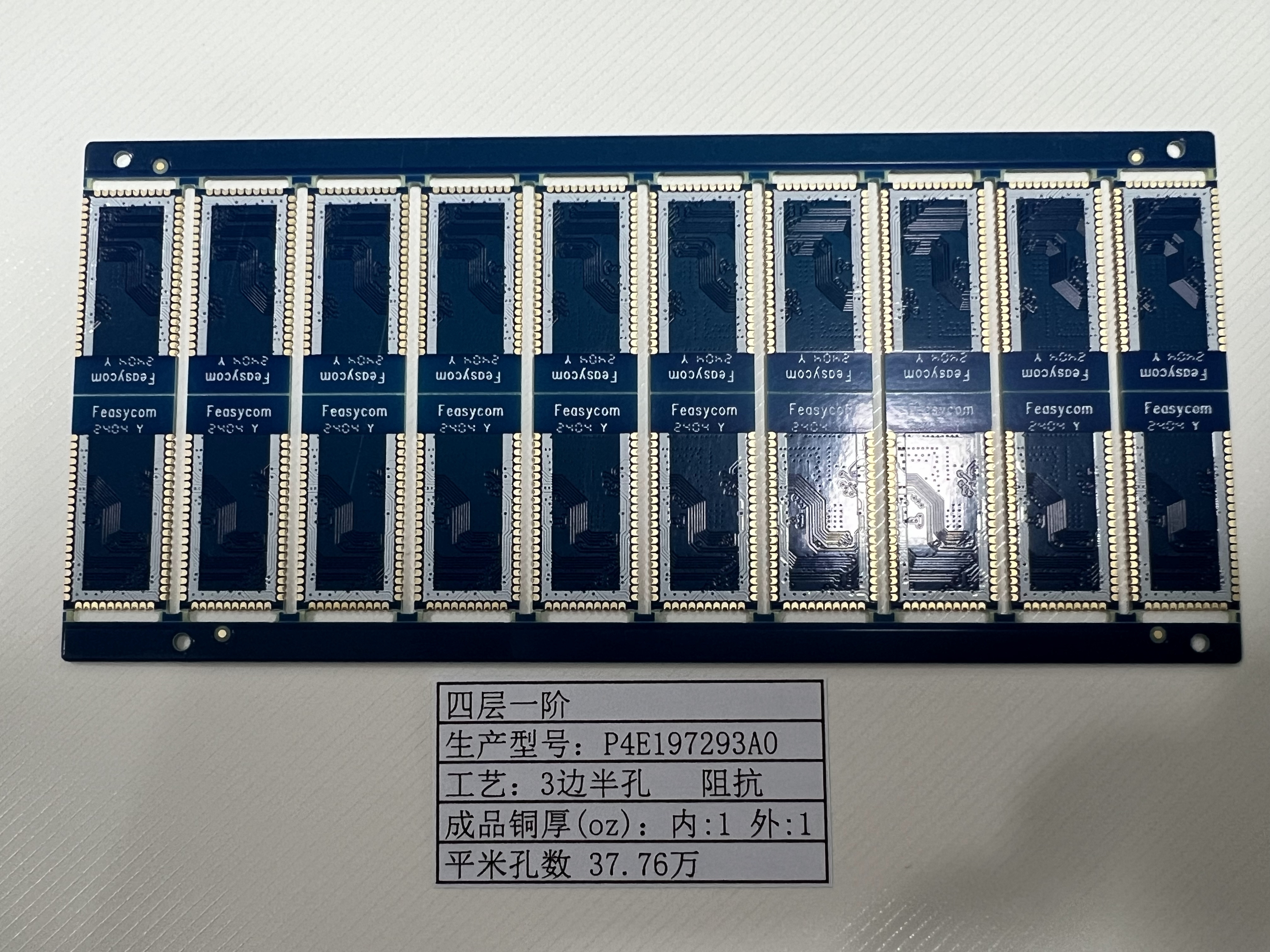
HDI PCBs use advanced technologies to achieve high density and compact layouts. The core structure relies on microvias, build-up layers, and specialized materials. Microvias are tiny, laser-drilled holes that connect two adjacent copper layers. These holes are much smaller than traditional plated through vias, saving valuable board space and allowing for more complex pcb design. A 10/4 mil microvia uses only a fraction of the area compared to a standard via, which helps engineers fit more connections into a smaller space.
Build-up layers form the foundation of high density interconnects. Manufacturers add these layers one at a time, using precise registration to align each layer. This process enables flexible stackup options, such as 2+N+2 or any-layer configurations. The use of advanced laminates and copper foils supports fine line widths and tight spacing, which are essential for modern pcb layout and routing.
HDI technologies also include semi-additive processes, which allow for trace lines as fine as 35μm. Automated optical shaping repairs defects before stacking, reducing scrap rates and improving yield. Electroless copper plating and laser drilling enhance via wall adhesion and reduce voids, leading to improved reliability and enhanced signal integrity. These innovations support high-speed signal transmission and thermal management, making HDI PCBs suitable for demanding applications.
HDI technologies enable manufacturers to achieve higher wiring density, better performance, and improved reliability in electronic devices.
PCB Design and Process
The pcb manufacturing process for HDI boards involves several precise steps. Engineers begin with detailed pcb design, focusing on stackup, routing, and component placement. They select the number of build-up layers and determine the best via structures, such as microvias, blind vias, or buried vias, to optimize density and signal flow.
The step-by-step process includes:
Design and Stackup Planning: Engineers create a detailed pcb design, specifying the stack-up and layer sequence. They plan the routing paths and select materials that support high density and thermal performance.
Material Preparation: Manufacturers prepare high-quality laminates and copper foils. These materials must meet strict tolerances for thickness and dielectric properties.
Laser Drilling and Via Formation: Laser drilling creates microvias with diameters under 150 micrometers. Electroless copper plating coats the via walls, ensuring strong electrical connections and reducing the risk of voids.
Build-up Layer Lamination: Each build-up layer is laminated and aligned with high precision. Laminate registration control achieves microvia-to-trace alignment within 25μm, which is critical for reliable connections.
Imaging and Etching: Semi-additive processes define fine trace lines and spaces, supporting complex routing and high density.
Automated Optical Inspection and Shaping: Automated systems inspect each layer and repair minor defects before stacking, reducing scrap and improving yield.
Final Assembly and Testing: The completed pcb undergoes electrical testing to verify connectivity and performance. Manufacturers may use flying probe tests or E-tests to ensure quality.
These advanced manufacturing techniques offer several efficiency gains:
Reduced power consumption by shortening signal paths and optimizing via structures.
Enhanced thermal management through thermal vias and heavy copper layers.
Improved manufacturing yield and reduced defects due to automated inspection and precise process control.
Faster time-to-market by minimizing trial-and-error cycles.
Applications of HDI PCB
HDI PCBs play a vital role in many industries that demand high density, compact size, and reliable performance. Their advanced structure and manufacturing process make them ideal for applications where space, speed, and reliability matter most.
Key applications include:
Mobile Devices: Smartphones and tablets rely on HDI PCBs for compact pcb layout, high-speed signal transmission, and support for advanced components like BGAs and fine-pitch connectors.
Aerospace and Defense: Avionics systems use HDI technology for lightweight, high-performance electronics that withstand harsh environments and require enhanced signal integrity.
Medical Equipment: Devices such as pacemakers, imaging systems, and portable monitors benefit from the small size, high density, and improved reliability of HDI PCBs.
Automotive Electronics: Advanced driver-assistance systems (ADAS), infotainment, and engine control units use HDI PCBs for robust performance and efficient routing in limited spaces.
Telecommunications: Network switches, routers, and 5G infrastructure depend on HDI PCBs for high-speed signal processing and controlled impedance routing.
The use of HDI PCBs in these industries leads to smaller, faster, and more reliable electronic products. Manufacturers achieve measurable gains in yield, cost reduction, and product performance by adopting high density interconnect and advanced pcb manufacturing techniques.
HDI technology transforms modern electronics by enabling compact, high-performance pcb solutions. LT CIRCUIT delivers reliable, advanced pcb products for demanding applications. Readers seeking innovation and quality in electronic design should explore LT CIRCUIT’s expertise and consider their hdi solutions for future projects.
FAQ
What makes HDI PCBs different from standard PCBs?
HDI PCBs use microvias and build-up layers. These features allow for higher wiring density and smaller device sizes.
Why do engineers choose LT CIRCUIT for HDI PCB manufacturing?
LT CIRCUIT provides advanced technology, strict quality control, and custom solutions. Engineers trust their expertise for reliable, high-performance HDI PCBs.
Which industries benefit most from HDI PCBs?
Mobile devices, automotive, aerospace, and medical equipment industries gain the most from HDI PCBs due to their compact size and superior performance.
See Also
Designing And Producing HDI PCBs With Multiple Layers
Understanding The Process Of Laser Hole Via Filling In HDI
Explore Cutting-Edge Techniques For HDI PCB Prototyping Now
Advantages Of LDI Exposure Machines In HDI PCB Circuit Production
Essential Design Factors For Reliable HDI High-Density Interconnects