What is a thick film ceramic PCB and how does it work
When you choose a thick film ceramic pcb, you’re working with a PCB that uses a ceramic substrate instead of the typical fiberglass base. This advanced design delivers exceptional thermal management. Thick film ceramic pcb technology allows ceramic materials to outperform traditional PCB options in both heat conductivity and temperature resistance, as shown below:
Material | Thermal Conductivity (W/mK) | Max Operating Temp | Use Case Example |
|---|---|---|---|
Ceramic (Aluminum Nitride, AlN) | 170–220 | 350°C+ | EV powertrain inverters, 5G base station amplifiers |
Ceramic (Aluminum Oxide, Al2O3) | 24–29 | 200°C | Industrial LED lighting, medical device sensors |
Ceramic (Beryllium Oxide, BeO) | 216–250 | 850°C | Aerospace radar systems, nuclear sensors |
Traditional FR4 | 0.3 | 130–150°C | Smartphones, laptops, home appliances |
Traditional Metal-Core (Al) | 10–30 | 150–200°C | Automotive infotainment, low-power LEDs |
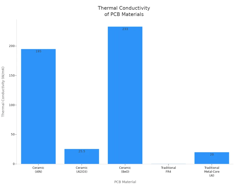
With a thick film ceramic pcb, your components stay cooler, making it the perfect choice for high-performance and demanding electronic applications.
Key Takeaways
Thick film ceramic PCBs use a ceramic substrate, offering superior thermal conductivity and temperature resistance compared to traditional PCBs.
These PCBs are ideal for high-performance applications in industries like aerospace, automotive, and telecommunications due to their durability and reliability in harsh conditions.
The manufacturing process allows for direct integration of resistors and conductors, saving space and enhancing electrical performance in compact designs.
Thick Film Ceramic PCB Overview
Definition and Structure
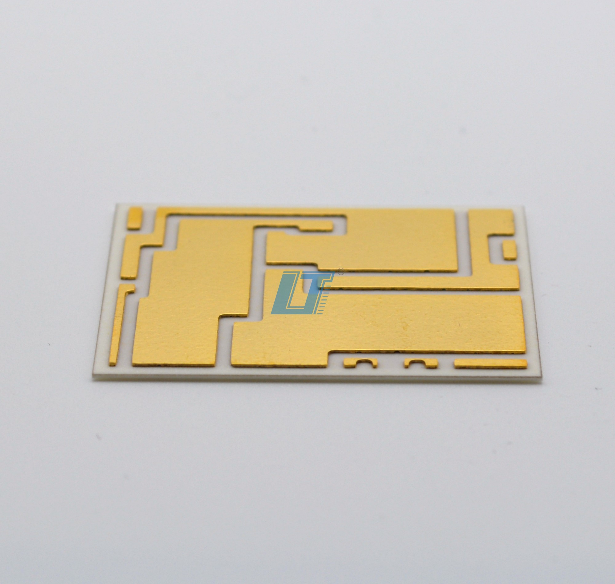
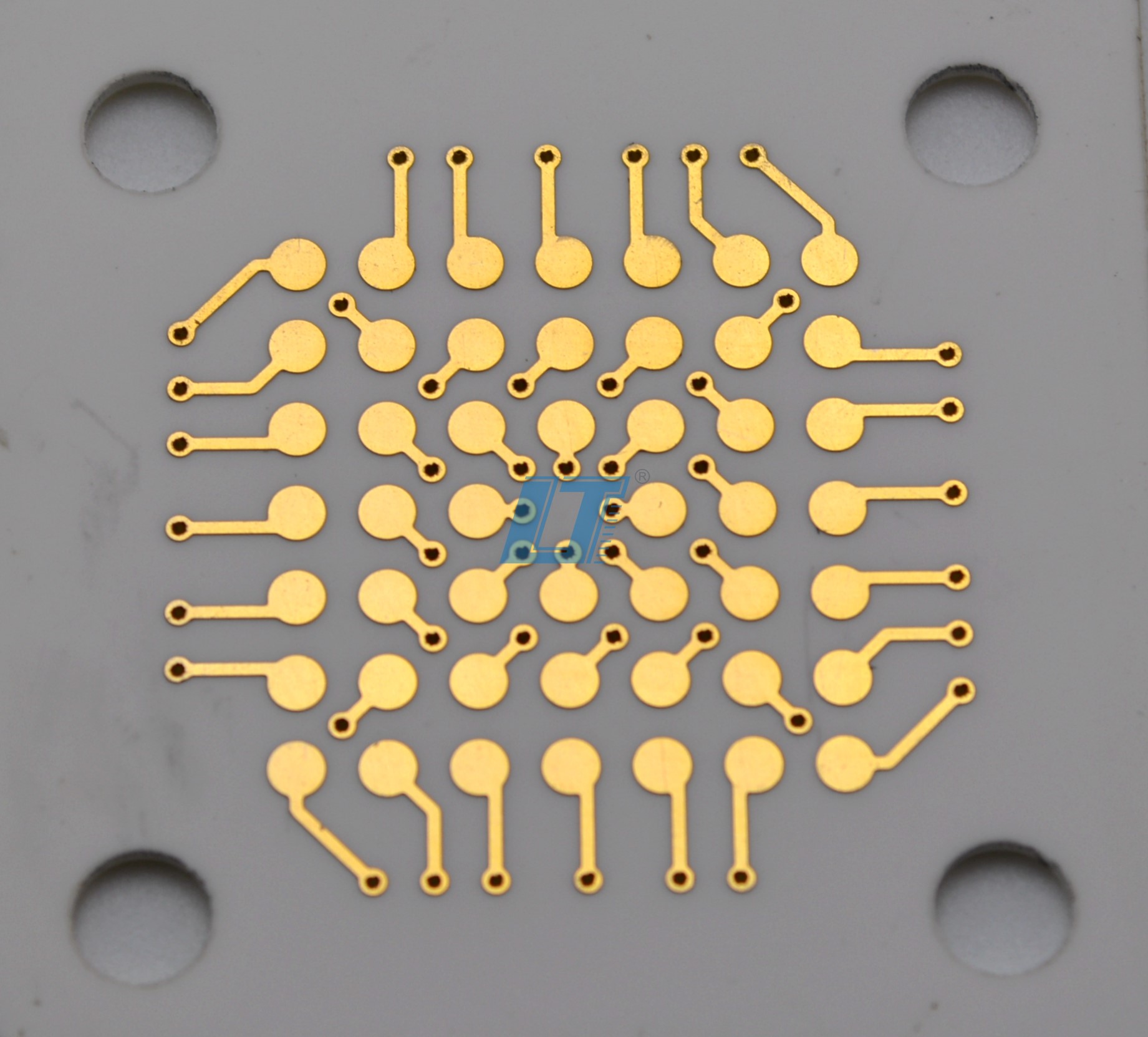
When you explore thick film ceramic pcb, you discover a printed circuit board that uses a ceramic substrate instead of the common organic base. This type of pcb stands out because it uses thick film technology, which means you get a thicker layer of conductive material compared to thin film or standard printed circuit boards. The thick film resistor ceramic pcb integrates resistors, conductors, and sometimes semiconductors directly onto the ceramic substrate. You benefit from a robust and durable structure that handles higher power levels and harsh environments.
Note: Thick film ceramic pcb technology uses screen printing and high-temperature sintering to deposit conductive, resistive, and dielectric materials onto the ceramic substrate. This process creates a circuit layer several micrometers thick, which gives you improved durability and power handling.
You can see how the structure of thick film ceramic pcb compares to traditional options in the table below:
Feature | Thick Film Ceramic PCB | Traditional PCB (FR-4) |
|---|---|---|
Substrate Material | Ceramic (Alumina, Aluminum Nitride) | Organic (FR-4) |
Thermal Conductivity | Superior | Moderate |
Mechanical Strength | High | Lower |
Manufacturing Process | Screen printing and firing | Etching and layering |
Design Flexibility | Direct printing of resistors | Limited |
Conductive Layer Thickness | Thicker (10-13 microns) | Thinner |
Electrical Performance | Higher dielectric losses | Lower dielectric losses |
Cost-effectiveness | Generally more cost-effective | Varies |
Key Features and Materials
You gain several advantages when you choose a thick film ceramic pcb. The ceramic substrate gives you high thermal conductivity, excellent chemical resistance, and strong mechanical strength. These features make ceramic pcb a top choice for demanding applications.
Here is a quick overview of the main materials used in ceramic pcb and their roles:
Material | Thermal Conductivity (W/m·K) | Features | Typical Applications |
|---|---|---|---|
Alumina (Al₂O₃) | 18–35 | Affordable, reliable | LEDs, consumer electronics, automotive circuits |
Aluminum Nitride (AlN) | 80–200+ | High thermal conductivity, CTE close to silicon | High-power electronics, aerospace systems, and MCPCB replacement in power modules |
Beryllium Oxide (BeO) | 209–330 | Exceptional thermal conductivity, but toxic | Military and aerospace ceramic PCB substrates |
Silicon Carbide (SiC) | 120–270 | Excellent electrical and thermal properties | High-power RF and power device ceramic PCBs |
Boron Nitride (BN) | 3.3–4.5 | Lightweight, chemically stable, low dielectric constant | RF circuits, heat-spreader ceramic PCBs |
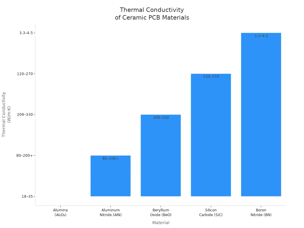
You will notice that ceramic pcb materials like AlN and SiC offer high thermal conductivity, which helps your components stay cool. The ceramic substrate also provides high-temperature resistance, making it ideal for high temperature ceramic pcb and low temperature ceramic pcb applications. You can rely on these materials for excellent electrical performance, mechanical strength, and chemical resistance.
Tip: The ceramic pcb substrate allows you to design circuits that operate at higher temperatures and in harsh environments, which is not possible with standard printed circuit boards.
How Thick Film Ceramic PCB Works
You benefit from thick film technology because it lets you print conductive, resistive, and dielectric layers directly onto the ceramic substrate. This process uses screen printing and high-temperature firing to create a robust printed circuit board. The thick film ceramic pcb can integrate resistors and capacitors right into the circuit, which improves functionality and saves space.
You can achieve a resistivity range from 10 Ω/□ to 100k Ω/□, which allows for precise voltage dividers and accurate signal processing.
The line resolution can reach 150 μm in prototypes and 300 μm in mass production, which reduces parasitic capacitance and improves signal integrity.
The thermal conductivity of ceramic pcb far exceeds that of traditional options. For example, AlN PCBs reach 180 W/mK, alumina PCBs reach 20 W/mK, while traditional PCBs only reach 0.3–0.4 W/mK. This high thermal conductivity means your thick film ceramic pcb can dissipate heat much faster, which is essential for high-power applications.
PCB Type | Thermal Conductivity (W/mK) |
|---|---|
AlN PCBs | 180 |
Alumina PCBs | 20 |
Traditional PCBs | 0.3–0.4 |
You also get high chemical resistance and low thermal expansion, which means your printed circuit board will last longer and perform better in tough conditions. The ceramic substrate protects against oxidation and environmental damage, so you can use your thick film ceramic pcb in automotive, aerospace, and industrial applications.
Advantages:
Outstanding thermal management
High durability and adaptability
Easy implementation of high-density tracing
Reliable performance in high-frequency and high-power applications
With these features, you can trust thick film ceramic pcb to deliver superior performance, especially when you need a printed circuit board that can handle heat, power, and harsh environments.
Manufacturing and Comparison
Manufacturing Process
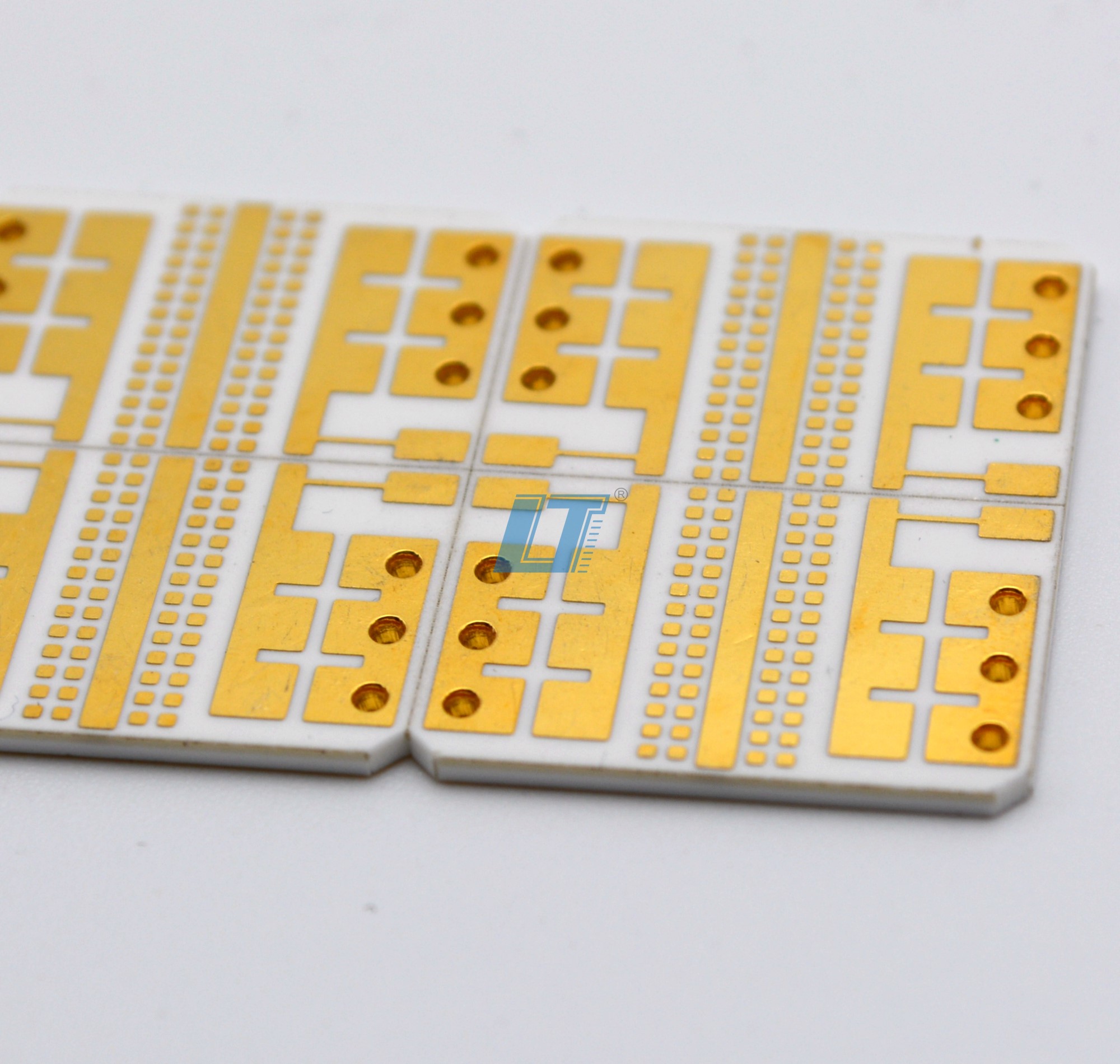
You can see how a thick film ceramic pcb is made by following a series of precise steps. The process starts with preparing the raw ceramic pcb materials. You cut and drill the substrate to match your design. After removing any blackening spots from laser drilling, you create a stencil for the circuit traces. You prepare conductive and resistive inks, then make a sample. You spread, dry, and fire the ink onto the substrate. Next, you print resistance ink and use a laser to trim resistors for accurate electrical performance. You add a glass glaze to protect the printed circuit board. Finally, you test, pack, and ship the finished pcb.
Raw material preparation
Substrate drilling and outline cutting
Blackening spot removal
Stencil creation for circuit traces
Conductive ink preparation
Sample making
Ink spreading, drying, and firing
Resistance ink printing and laser trimming
Glass glaze printing for protection
Product testing, packing, and shipment
The inks you use play a big role in conductivity and thermal management. Here is a table showing common ink materials and their properties:
Material | Conductor Width/Space | Performance Characteristics |
|---|---|---|
Gold | 8/8mil (0.20/0.20mm) | Good conductor, costly, poor solderability |
Silver | 8/8mil (0.20/0.20mm) | Lower cost, solderable, prone to migration under DC fields |
Platinum-Silver | 6/6mil (0.15/0.15mm) | Good adhesion, solderable, moderately good wire bonding |
Palladium-Silver | 8/8mil (0.20/0.20mm) | Good aged adhesion, solderable, wire bondable |
Resistance Value | 1Ω to several MΩ | Depends on carbon black type and ratio |
TCR | ±50ppm/°C to ±200ppm | Low TCR preferred for high-quality resistive paste |
The screen printing process introduces a glass phase into the metal slurry. This can reduce both electrical and thermal conductivity, which affects the performance of your ceramic pcb.
Thick Film vs. Thin Film PCBs
You may wonder how thick film ceramic pcb compares to thin film PCBs. Thick film technology costs less and works well for high-power applications like automotive and aerospace. Thin film PCBs suit microelectronics and RF devices, but they cost more, especially for prototypes.
Technology | Thick Film | Thin Film |
|---|---|---|
Cost | Relatively Low | High for prototype |
Application | High power devices | Microelectronics, RF |
Thick film ceramic pcb offers excellent mechanical strength and durability. You can rely on it in harsh conditions. It resists thermal cycling, mechanical stress, and moisture, which helps prevent failure in critical applications. Thick film circuits are flexible and cost-effective, making them ideal for high voltage, high current, and power electronics.
Advantages and Limitations
You gain several advantages with ceramic pcb. These printed circuit boards resist moisture and chemicals, which increases longevity. Their resistance to vibration, temperature extremes, and moisture ensures long-term reliability. You can use them in high-temperature applications because they withstand up to 850°C and offer high thermal conductivity.
Ceramic pcb can handle high temperatures and have excellent thermal conductivity, which boosts durability.
Feature | Thick Film Ceramic PCBs | Other PCB Types (e.g., FR-4) |
|---|---|---|
High-Temperature Tolerance | Up to 850°C | Fails under high temperatures |
Mechanical Strength | High resistance | Lower resistance |
Chemical Resistance | Impervious | Degrades with exposure |
Thermal Conductivity | Up to 170 W/m·K (AlN) | Lower conductivity |
Electrical Performance | Low TCR (±50 ppm/°C) | Higher drift |
Mechanical Durability | High rigidity | Prone to damage |
You should also consider the limitations. Ceramic pcb costs more due to expensive materials and complex manufacturing. The substrate is brittle, so it can break under stress. Design rules are more restrictive, and quality control is harder because of many processing steps.
Limitation | Description |
|---|---|
Higher Costs | |
Manufacturing Complexity | Specialized equipment, longer lead times |
Brittleness | Susceptible to failure under mechanical stress |
Design Constraints | Restrictive design rules |
Quality Control Challenges | Advanced inspection needed |
Tip: When you need a printed circuit board for demanding applications, ceramic pcb provides superior thermal management and durability, but you must weigh the cost and design constraints.
Applications of Thick Film Ceramic PCB
Typical Uses
You will find thick film ceramic pcb in many high-reliability applications where thermal management and electrical performance matter most. These boards support a wide range of uses because of their unique substrate and robust design. Here are some of the most common applications:
Aerospace: You can use these boards in satellites, missiles, and aircraft. They handle extreme temperatures and radiation.
Military: They play a key role in radar systems and fighter jets, offering high thermal and radiation resistance.
LEDs: You will see them in high-power LED modules, which benefit from excellent thermal conductivity and longer lifespan.
Automotive Electronics: These boards help manage heat in engine control modules and sensors, ensuring stable operation.
Telecommunications: They support reliable performance in communication devices and 5G infrastructure.
Semiconductor Packaging: You can rely on them for thermal conductivity and electrical insulation in semiconductor devices.
Power Modules: They keep inverters and converters cool for efficient operation.
Other Applications: You will also find them in medical implants, solar cells, and high-frequency power supplies.
Tip: The compact and dense structure of these boards allows you to design smaller devices without sacrificing performance.
Industry Adoption
Many industries have adopted thick film ceramic pcb for their thermal and reliability advantages. The table below shows how different sectors use these boards and the benefits they gain:
Industry | Application Description | Adoption Metrics |
|---|---|---|
Aerospace | Navigation, flight control, satellite components | 30% longer operational lifespan, better signals |
Medical Imaging | MRI and CT scanners, high-frequency signal transmission | 20% less downtime, improved image resolution |
Automotive | Electric vehicle inverters, battery management | 15% yearly adoption growth |
Telecommunications | 5G infrastructure, radar systems | 25% higher data throughput |
Industrial Automation | Power converters, motor controllers | 10% annual growth in use cases |
You will notice that the market for these boards continues to grow. Experts project the global market to rise from $2.8 billion in 2024 to $4.9 billion by 2033, with a steady annual growth rate. This trend shows that more industries value the advantages of thermal management, miniaturization, and high-reliability applications. When you need a pcb that delivers strong electrical performance and withstands harsh environments, thick film ceramic technology stands out as a top choice.
You gain several advantages with thick film ceramic PCBs:
High thermal tolerance prevents heat-related damage.
Low dielectric loss supports high-frequency use.
Superior reliability in harsh conditions.
Future trends in electronics, electric vehicles, and 5G networks make these PCBs a smart choice for your most demanding projects.
FAQ
What makes thick film ceramic PCBs better for high-temperature environments?
You get higher thermal conductivity and temperature resistance. Ceramic substrates help your board stay cool and reliable in demanding conditions.
Can you integrate resistors directly onto a thick film ceramic PCB?
Yes, you can print resistors onto the ceramic substrate. This saves space and improves electrical performance for your design.
Are thick film ceramic PCBs suitable for miniaturized devices?
Feature | Suitability |
|---|---|
High Density | ✅ |
Small Footprint | ✅ |
Reliable | ✅ |
You can use these PCBs in compact electronics without sacrificing durability.
See Also
The Superior Heat Dissipation Properties of Ceramic PCBs
A Comprehensive Overview of Multilayer Ceramic PCB Production
Ceramic PCBs: Key Applications Across Various Industries Today