Why Controlled Impedance Is Essential for High-Speed PCB
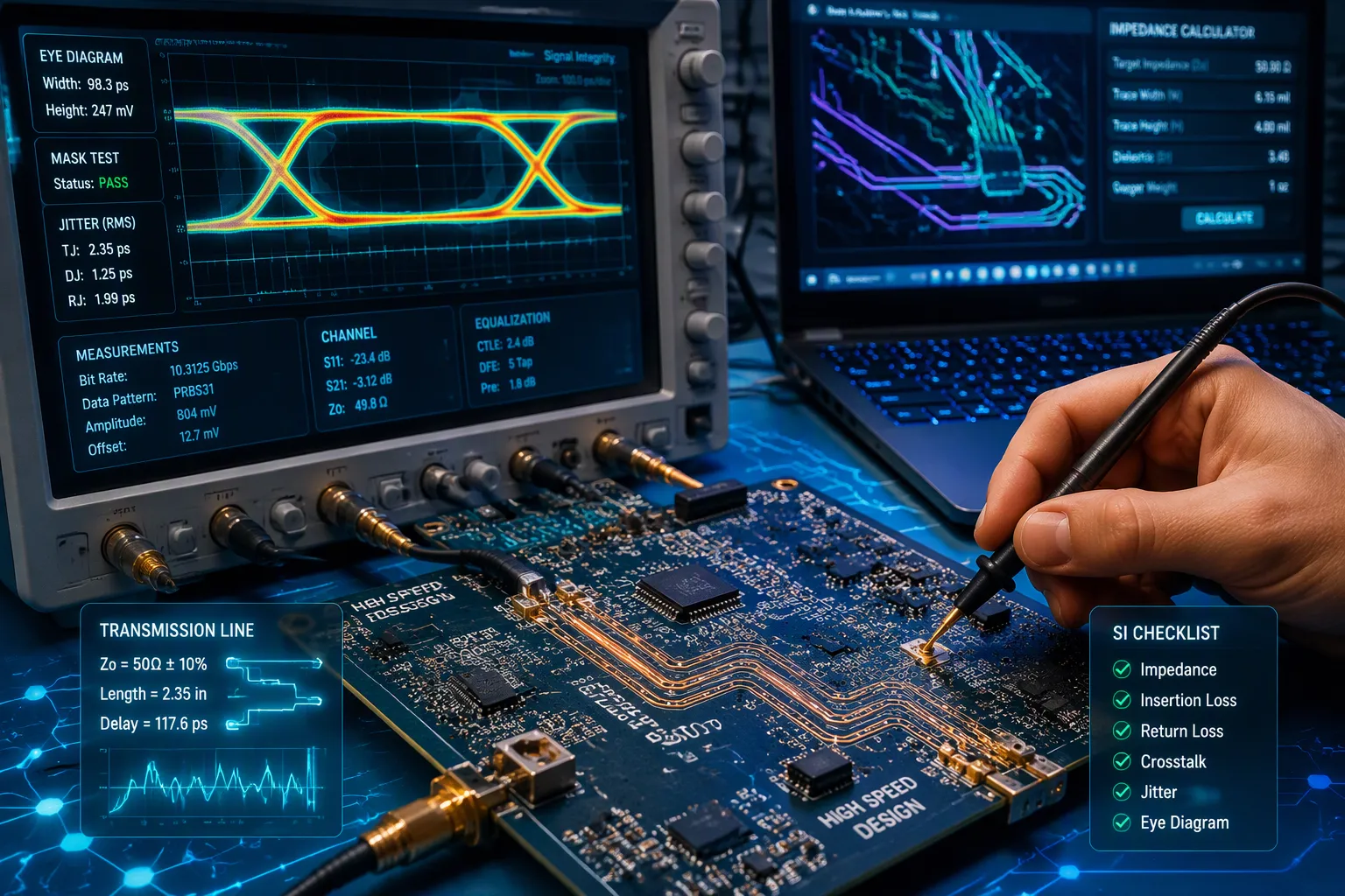
Your prototype passes functional tests, but final validation exposes the truth: intermittent bit errors on the data bus, excessive ringing on every clock edge, and radiated emissions above the limit. A termination tweak fixes one symptom. Another appears. The true culprit is a signal integrity failure, not random noise. Controlled impedance solves this by matching each trace's characteristic impedance to a specified target, commonly 50 Ω or 100 Ω. With high-speed edge rates, every trace behaves as a transmission line. Uncontrolled impedance creates reflections, timing errors, crosstalk, and EMI. You can prevent this by following a practical engineering path—understanding the physics, setting targets in layout, then verifying the manufactured pcb.
Key Takeaways
Controlled impedance matches trace impedance to a target, preventing signal reflections and ensuring reliable high-speed performance.
Fast edge rates turn PCB traces into transmission lines, requiring impedance control to avoid signal integrity issues.
Impedance mismatches cause reflections, ringing, and timing errors, which can lead to data corruption and certification failures.
Key design factors include dielectric properties, trace geometry, and reference planes, all affecting impedance.
A practical workflow involves identifying critical nets, planning stackup, and routing differential pairs symmetrically.
Verification after manufacturing uses test coupons and TDR/VNA measurements to confirm impedance targets are met.
Controlled impedance reduces prototype spins, debug time, and ensures reliable system performance, saving costs.
Always consult component datasheets and fabricator capabilities to set appropriate impedance targets and tolerances.
Why High-Speed PCB Design Needs Controlled Impedance
Controlled impedance means matching each trace's characteristic impedance to a specified target value, such as 50 Ω for single-ended signals or 100 Ω for differential pairs. This matching ensures the signal travels from driver to receiver without disruptive reflections. In high-speed PCB design, this discipline separates a working prototype from a failing product.
Fast Edge Rates Turn Traces Into Transmission Lines
Modern digital signals switch at incredible speeds. Frequencies above 100 MHz often fall into the high-speed category because they carry shorter wavelengths and faster edge rates. Signal bandwidth, including harmonics reaching into the gigahertz range, can push a design into high-speed territory. When rise times shrink, the signal's high-frequency content grows, and your traces stop behaving like simple wires.
A useful rule of thumb helps you decide when a trace becomes a transmission line. For digital signals, the critical conductor length is one-sixth of the physical length occupied by the rising or falling edge, whichever is faster. Conductors longer than this threshold behave as transmission lines. The physical length of the edge depends on the rise time and the propagation velocity, which in turn depends on the dielectric constant of your PCB material. You can also think of it this way: the critical length is the line length over which the signal propagation time equals half of the fastest rise time. If the signal travels from the source over that length and returns in a total time equal to the rise time, the trace acts as a transmission line.
As signal switching speeds continue to increase, PCB designers must pay closer attention to the impedance characteristics of printed circuit board traces. Short transition times and high-frequency operation mean PCB traces behave like transmission lines, not ideal conductors. ... As signal rise times continue to decrease, the number of traces requiring impedance control will naturally increase.
The table below summarizes the key thresholds you should monitor.
Parameter | Value/Range | Implication for Controlled Impedance |
|---|---|---|
High-speed signal frequency range | 50 MHz to 3 GHz | Signals in this range are considered high-speed and require impedance control |
Transmission line criterion | Trace length > 1/10 of wavelength | Traces exceeding this threshold must be treated as transmission lines, making controlled impedance essential |
Rise time effect | Shorter rise times increase high-frequency harmonics | Decreasing rise times cause ringing, crosstalk, reflections, and impedance mismatch, necessitating controlled impedance |
A Fixed Target Value Keeps the Signal Path Predictable
A stable target impedance, such as 50 Ω, delivers predictable propagation delay and signal amplitude. When impedance stays uniform between the driver and the transmission line, reflections stay minimal. Abrupt impedance changes at interfaces or connectors cause signals to reflect back toward the source, producing overlapping transitions, timing uncertainty, and skew. High-speed interfaces such as DDR, Ethernet, and USB have strict impedance requirements to ensure reliable data transfer. DDR memory systems operate at high frequencies and rely on precise timing, so impedance mismatch can cause reflections, timing errors, and data corruption. For DDR designs, single-ended traces typically require 50 Ω characteristic impedance, while differential pairs such as clock signals often need 100 Ω. Ethernet interfaces, especially Gigabit Ethernet or 10GbE, use differential signaling and generally require 100 Ω impedance for differential pairs.
Different interfaces demand different targets. PCI Express uses 90 Ω differential and 50 Ω single-ended. USB 2.0 and USB 3.0 both use 90 Ω differential and 50 Ω single-ended. LVDS LCD panels use 100 Ω differential and 55 Ω single-ended. HDMI and DVI use 90 Ω differential and 50 Ω single-ended. The chart below compares these nominal values across common interfaces.
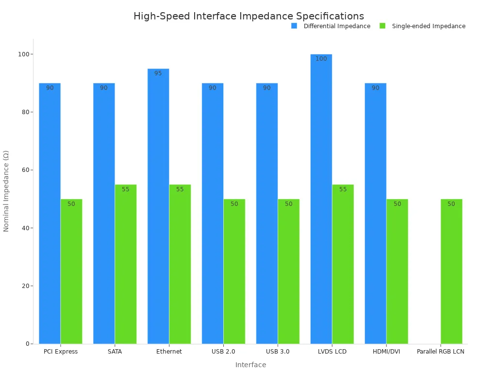
When controlled impedance is specified, the manufacturer aims for ±10% tolerance using defined processes. Selecting an appropriate stackup variant ensures both impedance targets and phase consistency remain achievable within practical manufacturing limits.
Impedance Matching Prevents Reflections at the Receiver
Impedance matching is the core defense against signal reflections. When the transmission line impedance does not match the source or load, signal energy reflects back toward the source. These reflections cause signal distortion, ringing, overshoot, and undershoot, which degrade signal quality and lead to data errors or communication failures.
Consider a 50 Ω source driving a 75 Ω load. The load reflection coefficient is calculated as (75 − 50) / (75 + 50) = 25 / 125 = 0.2. Because the result is positive, the reflected wave arrives in phase with the incident wave at the receiver and adds to it, producing overshoot. Impedance mismatches like this can reflect up to 20% of the signal energy back, causing ringing. On the source side, if the source resistance equals the line impedance, the reflection coefficient is zero. The returning wave is absorbed rather than re-reflected, so repeated bouncing and ringing are avoided. When the source is not matched, the wave continues bouncing between the two ends and rings out as energy is absorbed at the source and lost in the interconnect.
Properly matching the characteristic impedance between transmission lines and components or connectors minimizes reflections and supports efficient signal propagation. A stable impedance target like 50 Ω contributes to more predictable timing and signal amplitude by reducing reflection-related distortion and delay variation. This is why impedance control is not optional in high-speed PCB design—it is the foundation of reliable signal integrity.
Trace Impedance Control Prevents Signal Integrity Failures
Signal Reflections Cause Overshoot, Undershoot, and Ringing
When a traveling wave meets an impedance change, part of the signal energy bounces back toward the source. This reflection acts like an echo in a pipe. The reflection coefficient determines the reflected amplitude: an open circuit reflects positively, a short circuit reflects negatively, and a matched impedance produces no reflection. You calculate this coefficient as rho = (ZL - Z0) / (ZL + Z0), where Z0 is the source transmission line impedance and ZL is the impedance at the discontinuity.
Common sources of these discontinuities include vias, connectors, test pads, and abrupt trace width changes. An unterminated 100-ohm differential pair reflects half the energy back. The round-trip propagation delay, roughly 150 ps per inch in FR4, sets the ringing period. Multiple discontinuities compound the problem because reflections sum into unpredictable waveforms. These reflected waves combine with the original signal, appearing on an oscilloscope as overshoot, undershoot, or ringing. In multi-layer boards, stackup variations change impedance along the trace, making reflections more likely.
Timing Errors Shrink the Eye Pattern
Eye height shows how efficiently the signal distinguishes between high and low logic levels, representing the signal-to-noise ratio. Eye width indicates sampling accuracy at a specific timing interval, reflecting timing margin. Signal integrity weakens when jitter and noise cause deviations from ideal signal edges.
Impedance mismatches inside a package create reflections at the discontinuity. These reflections interfere with the forward-propagating signal and cause significant amplitude and timing degradation. In one comparison, an impedance-matched structure achieved an eye width of 17.81 ps and eye height of 49 mV. An impedance-mismatched channel dropped to 16.56 ps eye width and 39 mV eye height. This degradation stems from increased insertion loss, larger residual ISI, and amplified timing uncertainty. As total jitter approaches 0.5 unit interval, the timing margin disappears entirely.
Crosstalk and EMI Threaten Certification
Uncontrolled impedance increases bit error rates and degrades communication quality. It also reduces noise margins, making your high-speed pcbs more susceptible to crosstalk. Broken or split return paths increase loop inductance and cause high-speed traces to radiate, creating an additional EMI/EMC failure mode.
Regulatory limits leave little room for error. CISPR 32 Class B and FCC Part 15 Sub B tests do not forgive layout oversights; even a 3 dB spike can fail certification. On a 10-layer PCIe Gen4 board, radiated emissions exceeded CISPR limits by 6 dB at 400 MHz. Removing via stubs and tightening decoupling placement resolved the failure. Under CISPR 32, radiated emissions are limited to 40 dBµV/m from 30–230 MHz and 47 dBµV/m from 230–1000 MHz. Fast switching edges generate energy into the GHz range, and impedance mismatches at vias and connectors create reflections that amplify radiated emissions above these thresholds.
Key Variables That Drive Controlled Impedance Design
Dielectric Properties and Stackup Set the Baseline
The dielectric constant of your laminate sets the foundation for every impedance target. FR-4 has a dielectric constant of approximately 4.5. High-frequency laminates such as Rogers and Teflon offer lower values between 2.2 and 3.0, which help you achieve higher signal speed and controlled impedance. A lower dielectric constant increases signal transmission speed and supports higher characteristic impedance. When the dielectric constant rises, signal propagation slows and you must narrow traces to hit a given impedance target.
Dielectric thickness between a signal trace and its reference plane directly influences impedance. Thinner dielectric layers decrease impedance by bringing traces closer to the reference plane. Thicker layers increase it. You adjust this thickness to reach your desired impedance values. Resin content affects both final thickness and dielectric constant, and higher thickness generally lowers the dielectric constant. For the same material, different core thicknesses and prepreg types have different resin contents and thus different dielectric constants. Stable dielectric constant across frequencies makes a laminate suitable for controlled impedance boards.
Trace Width, Height, and Copper Roughness Change Impedance
Trace width and spacing define the inductive and capacitive balance of your pcb trace geometry. Wider traces lower impedance by increasing capacitance, and narrower traces raise it. A change of 0.025 mm in trace width can alter impedance by 5–6 ohms. Copper weight, typically 1 oz or 2 oz, influences both electrical characteristics and total board thickness. One ounce copper is 0.035 mm thick, and the effective-width correction adds 0.03–0.05 mm to the physical trace width. A copper-etch tolerance of ±0.025 mm can cause impedance variations of ±3–5 Ω.
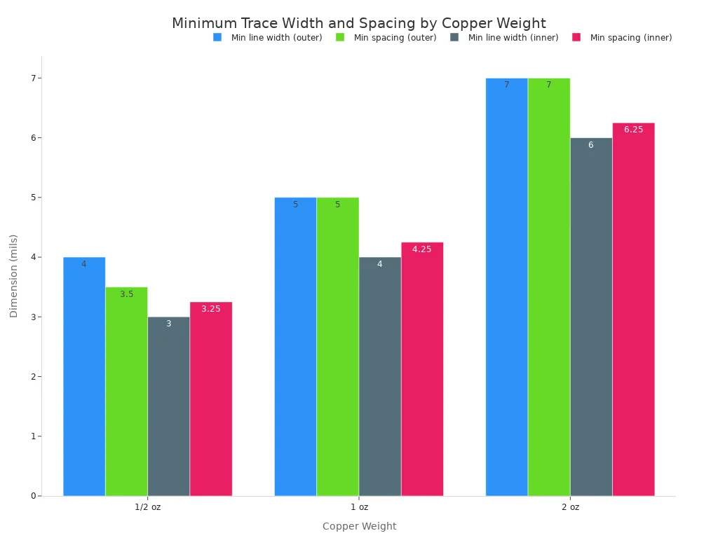
Copper foil roughness increases the effective dielectric constant and slightly alters impedance. Higher roughness improves adhesion but increases high-frequency attenuation from skin-effect loss, which indirectly affects controlled impedance at gigahertz frequencies. Low-profile foil is favored when signal integrity is critical. Copper roughness is characterized by quantitative metrics such as Ra, Rz, and Sq under ISO 4287/25178 and IPC-TM-650. The chart below compares minimum trace width and spacing by copper weight.
Reference Planes and Manufacturing Tolerances Add Variation
Above roughly 1 MHz, return current follows the path of least inductance directly beneath the signal trace on the nearest reference plane. A slot in the ground plane forces the return current to detour around it, dramatically increasing loop area. At 1 GHz even a 2 mm slot can degrade EMC performance by more than 20 dB. Through-hole via anti-pads create clearance voids in ground planes, and dense via fields can produce Swiss-cheese ground planes with significantly increased impedance. Maintain a 3:1 trace-to-plane spacing ratio to contain fields and preserve tight coupling. Stitching vias every lambda/20 along plane edges and splits help maintain continuity.
Manufacturing tolerances add another layer of variation. Trace width should be controlled within approximately ±20% to improve impedance control. Standard digital circuits often accept ±10% impedance tolerance, while high-speed digital and RF circuits typically require ±7% or even ±5%. Aerospace and telecommunications applications often demand stricter control. Lamination temperature, pressure, and vacuum level all affect dielectric thickness uniformity. A thinner laminated area can increase local impedance and cause reflections in high-speed circuits. Consistent dielectric constant, controlled resin content, and low copper roughness are essential for maintaining precise impedance control.
A Practical Workflow for Impedance Control in PCB Layout
You now understand the physics and the failure modes. The next step is execution. A disciplined workflow turns impedance targets into manufacturable geometry. Follow these steps to move from concept to a routed board that meets specification.
Identify Impedance-Critical Nets and Set Targets
Start by annotating every net that carries high-speed signals. Your schematic capture tool lets you assign net classes before layout begins. Mark single-ended nets that need 50 Ω and differential pairs that require 90 Ω or 100 Ω. Consult component datasheets and interface specifications for exact values.
Common interfaces have well-defined targets. USB 2.0 and USB 3.x require 90 Ω differential impedance. PCIe specifies 85 Ω differential. DDR4 memory buses use 40 Ω single-ended traces and 80 Ω differential pairs. HDMI requires 100 Ω differential impedance. Failure to meet these targets within the allowed tolerance—typically ±10%—directly causes signal integrity failures.
After component placement, set the impedance profile in your PCB design rules. This ensures routing uses the correct width, clearance, and spacing to maintain controlled impedance during high-speed routing. Define the target impedance for critical traces using industry standards or component datasheets. Select PCB materials and stackup, considering dielectric constant, layer thickness, and copper weight. Work with your manufacturer to define a stackup that supports consistent impedance.
Optimize Stackup and Trace Parameters Before Routing
Plan the PCB stackup before routing. Each high-speed signal layer must reference a continuous, uninterrupted ground plane. Power and ground planes should be closely coupled with symmetrical construction to reduce warpage.
Determine controlled impedance targets during stackup planning. Trace width, dielectric thickness, copper weight, and laminate Dk collectively define impedance. Calculate trace width and spacing using your fabricator's exact parameters—real substrate Dk and prepreg thickness data—rather than generic field-solver assumptions. This accounts for manufacturing tolerances such as ±10% controlled impedance tolerance.
Define and implement design constraints in your PCB design software. Set target impedance, differential pair spacing, skew budgets, trace width and clearance, length-matching tolerances, via restrictions, and manufacturing limitations. Verify the stackup matches impedance calculations. Confirm controlled impedance traces use correct width and spacing. Clearly specify impedance requirements in fabrication notes.
A symmetrical six-layer stackup with signal, ground, power, signal, ground, and signal layers supports single-ended DDR signals at 50 Ω and differential clock pairs at 100 Ω. Each high-speed routing layer sits adjacent to a reference plane.
Route Differential Pairs Symmetrically With Solid Return Paths
Route high-speed differential pair signal traces with symmetry. Both traces in a pair must have equal length and consistent spacing. Any asymmetry creates skew, which converts differential signals into common-mode noise and degrades signal integrity.
Maintain a solid return path beneath every high-speed trace. Above roughly 1 MHz, return current follows the path of least inductance directly beneath the signal trace on the nearest reference plane. A slot in the ground plane forces the return current to detour, dramatically increasing loop area. At 1 GHz even a 2 mm slot can degrade EMC performance by more than 20 dB.
Control Spacing and Via Discontinuities
Keep differential pair spacing constant along the entire route. Spacing changes alter differential impedance and cause reflections. When you must transition between layers, use via transitions that preserve impedance. Back-drill via stubs on thick boards. Via stubs act as stubs that reflect energy at high frequencies.
Place ground stitching vias near signal vias to provide a continuous return path. Route both traces of a differential pair through vias together. Avoid routing one trace through a via while the other remains on the same layer. This creates a discontinuity that destroys differential impedance.
For PCIe Gen4 and Gen5 designs, back-drilling is mandatory. These interfaces require low-loss PCB materials with Dk below 4.0 and Df below 0.005. Skew must stay below 1 ps for Gen5. USB 3.x requires AC coupling capacitors and strict length matching with intra-pair skew below 2 mil.
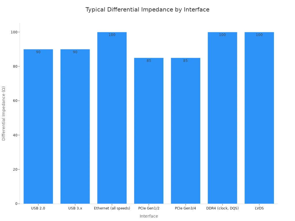
Always derive the actual trace width and gap from your fabricator's stackup using a field solver. These values are starting points, not universal rules. DDR4 single-ended impedance values of 40–50 Ω are a starting point only. The correct target is controller-dependent. Your SoC or CPU hardware design guide specifies the required impedance and tolerance. That document takes precedence over any generic recommendation.
USB 3.x specifications define 90 Ω ±7% as the standard differential impedance target. Some processor vendors specify 85 Ω in their hardware design guides for USB 3.x and PCIe lanes. That 85 Ω value is a platform-specific deviation, not a general recommendation. Always check your SoC or host controller's hardware design guide.
Verifying Impedance Targets After Manufacturing
You have routed your board with controlled impedance traces and approved a stackup design. Now you must prove the fabricated pcb meets specification. Verification closes the loop between design intent and physical hardware.
Specify Tolerances and Confirm Fabricator Capabilities
Define your acceptance tolerance before you release the order. A ±10% impedance tolerance is common for many controlled-impedance PCB designs. Some applications require tighter tolerances, such as ±8% or ±5%, but tighter requirements should be reviewed with the PCB manufacturer because they may affect materials, stackup, manufacturing controls, testing, cost, and lead time.
A ±10% impedance tolerance is common for many controlled-impedance PCB designs. Some applications require tighter tolerances, such as ±8% or ±5%, but tighter requirements should be reviewed with the PCB manufacturer because they may affect materials, stackup, manufacturing controls, testing, cost, and lead time.
Cost rises sharply as tolerance tightens. Standard pricing covers ±10% for most digital designs. A ±7% tolerance adds 10–15% for high-speed SerDes and DDR4/5. A ±5% tolerance adds 15–30% for RF, precision timing, and DDR5. Specialized RF and test equipment may demand ±3% at 40–60% or more. Tighter trace width tolerance is the dominant variable, followed by thinner prepreg thickness tolerance, consistent Dk across the panel, and in-process impedance monitoring.
Validate With Coupons and TDR/VNA Measurements
An impedance test coupon is a specially designed structure etched onto a production panel that replicates critical impedance-controlled traces from the actual PCB design. Its primary purpose is to verify that the manufactured board's trace impedance matches the design target, accounting for real stackup variations such as core and prepreg thickness differences. Coupons are typically designed as stripline or microstrip pairs with specific lengths to minimize end effects, and they are positioned away from panel edges to avoid warping influences. IPC standards define coupon geometries and test procedures, ensuring consistent and repeatable impedance verification across manufacturing lots.
Measurement Method | Principle | Advantages | Typical Use Case |
|---|---|---|---|
TDR (Time Domain Reflectometry) | Sends a fast-rising step pulse (rise time < 35 ps) down the trace and analyzes reflected waveform to determine impedance versus position. | Pinpoints localized impedance mismatches along a trace; ideal for debugging. | Verifying 50-ohm single-ended traces or 100-ohm differential pairs in high-speed designs; quick production scans. |
VNA (Vector Network Analyzer) | Measures scattering parameters (S-parameters) over a frequency spectrum (e.g., 10 MHz to several GHz) to derive impedance. | High precision for complex designs with varying frequencies; provides broadband validation. | Testing impedance in RF circuits where consistent 50-ohm match is required across wide bandwidth; detailed frequency analysis. |
Use TDR to Detect Reflection Discontinuities
TDR measurements are performed by applying a fast-rise-time pulse to the PCB trace and observing the reflected waveform to identify impedance changes caused by defects such as opens, vias, stubs, or width variations. For differential transmission lines, TDR characterizes the pair by driving it in odd, even, or differential modes and analyzing the resulting reflections. The odd-mode impedance is measured across one line while a complementary signal drives the other; differential impedance is measured across the two lines with the pair driven differentially and is double the odd-mode impedance. The even-mode impedance is measured across one line while an equivalent signal drives the other, and common-mode impedance is half of the even-mode impedance. Modern TDR instruments automatically compare incident and reflected amplitudes to provide direct readouts of impedance, reflection coefficient, and time for both common mode and differential impedance.
Use VNA for Frequency-Dependent Verification
A VNA measures S-parameters over a frequency range, such as 10 MHz to several GHz, to calculate impedance across a spectrum. This method offers high precision for RF designs that require a consistent 50-ohm match across wide bandwidth. TDR is favored for quick production scans, while VNA provides detailed frequency analysis for complex designs. Combined use gives you both time-domain and frequency-domain confidence.
Review Impedance Reports Before Assembly
Request proof before bare boards enter assembly. Discovering a wrong stackup or missing report after assembly is expensive. Check that the lot or job ID matches your PO or supplier job. Confirm the drawing revision matches your released files and stackup revision. Verify the target and tolerance match your drawing note or RFQ. Confirm the measured value falls inside the accepted range. Check the coupon reference identifies the tested layer pair, structure, or net. Compare the approved stackup against the report. Treat a missing report as an open question. An out-of-tolerance result requires an engineering deviation or risk acceptance before SMT.
The Business Case for Controlled Impedance
Controlled impedance is not just an engineering preference. It is a financial decision. When you design with impedance targets in mind, you avoid the hidden costs of signal integrity failures. These costs include repeated prototype builds, extended debug sessions, and delayed product launches.
Fewer Prototype Spins and Faster Debug
Strong signal integrity through controlled impedance design translates into fewer design iterations and faster time to market. Early simulation and manufacturer consultation catch issues before you cut copper. This saves time and reduces costly design iterations. An automotive supplier used controlled impedance boards for ADAS radar front-end designs and reduced signal-integrity debug cycles. You can achieve similar results by simulating electrical performance before physical prototyping. This practice identifies impedance mismatches early and cuts down on physical prototype iterations.
Cleaner Timing Margins Mean Reliable System Performance
A wide, tall eye diagram indicates a robust link. A closed eye signals high bit-error-rate risk and impending product-level failures. Controlled impedance routing prevents reflections and produces a cleaner eye, which reduces transmission errors that could otherwise appear as field faults. The table below summarizes how design practices affect reliability.
Design practice | Effect on timing margins | Effect on system reliability |
|---|---|---|
Controlled impedance design | Prevents reflections that distort waveforms and shift timing | Avoids intermittent signal faults that cause returns and field repairs |
Impedance matching and termination | Reduces ringing, overshoot, and double-clocking | Preserves timing margins and prevents logic errors |
Balanced differential routing | Delivers clean eyes and stable timing in noisy environments | Improves noise immunity and reduces intermittent field issues |
Verification with eye diagrams and impedance plots | Confirms margin before boards are released | Reduces bring-up and certification risk |
A Final Review Checklist for Impedance Targets
Before you release your high-speed pcbs for controlled impedance fabrication, run a structured review. This checklist prevents expensive mistakes.
Verify the stackup has been reviewed with the PCB manufacturer.
Confirm target impedance is defined for all high-speed nets.
Ensure trace width and spacing remain within fabrication tolerance.
Check that critical signals have continuous return paths.
Validate eye diagrams and jitter budgets through post-layout simulation.
Provide controlled-impedance values and tolerances in the fabrication package.
Complete a final DFM review.
Verify Targets, Stackup, Layout, and Test Data
Confirm that impedance is controlled consistently across layers. Minimize impedance discontinuities at vias and connectors. Define test coupons if required. Ensure the stackup is symmetric and high-speed signal layers sit adjacent to solid reference planes. Review simulation results and document risks with mitigation plans. Freeze the design only after all items pass.
These steps turn impedance control from a theoretical concern into a repeatable process. You protect your schedule, your budget, and your product reputation.
Controlled impedance is not just layout theory. It determines whether your high-speed system works reliably in the field. Designing for impedance early prevents expensive field failures and certification rework. Share your stackup, tolerances, and test requirements with your fabricator. This partnership makes controlled impedance a shared goal.
Add controlled impedance review to your design checklist. Validate it with TDR data before release. You protect your schedule, your budget, and your product reputation. A pcb that meets impedance targets delivers cleaner timing margins and fewer surprises during validation.
FAQ
When does a trace need controlled impedance?
A trace becomes a transmission line when its length exceeds one-sixth of the physical length of the fastest signal edge. Conductors longer than this threshold require impedance control. Shorter traces may not need it, but faster rise times push more nets into this category.
What target values should you assign to common interfaces?
USB 2.0 and USB 3.x use 90 Ω differential. PCIe specifies 85 Ω differential. DDR4 memory buses use 40 Ω single-ended and 80 Ω differential pairs. HDMI requires 100 Ω differential. Always confirm these values against your component datasheet and controller design guide.
How tight should your impedance tolerance be?
A ±10% tolerance suits most digital designs. High-speed SerDes and DDR4/5 often need ±7%. RF and precision timing circuits may require ±5%. Tighter tolerances raise cost and lead time, so review them with your fabricator before release.
What causes impedance discontinuities on a pcb?
Vias, connectors, test pads, and abrupt trace width changes create discontinuities. Slots in reference planes force return current to detour, increasing loop area. Back-drill via stubs on thick boards. Keep spacing constant along differential pairs to avoid reflections.
How do you verify impedance after fabrication?
Request impedance test coupons etched onto the production panel. Use TDR to detect localized reflection discontinuities along a trace. Use a VNA for frequency-dependent verification across a spectrum. Review the impedance report before assembly and treat missing data as an open question.
Why does copper roughness matter for impedance?
Copper foil roughness raises the effective dielectric constant and slightly shifts impedance. Higher roughness also increases high-frequency attenuation from skin-effect loss. Low-profile foil is preferred when signal integrity is critical. Roughness is characterized under IPC-TM-650 and ISO 4287/25178.
What happens if you skip controlled impedance on a high-speed pcb?
Uncontrolled impedance causes reflections, ringing, overshoot, and timing errors. Eye patterns shrink, crosstalk rises, and radiated emissions may exceed CISPR 32 or FCC Part 15 limits. These failures often appear only during final validation, forcing expensive redesigns and delayed launches.
How do you set up impedance control in layout?
Annotate impedance-critical nets in your schematic. Assign net classes with target values before routing. Plan the stackup with your fabricator using real substrate data. Route differential pairs symmetrically with continuous reference planes. Define design rules for width, spacing, and via transitions.
