Why Do Most PCB Use 50, 90, or 100 Ohms for Impedance
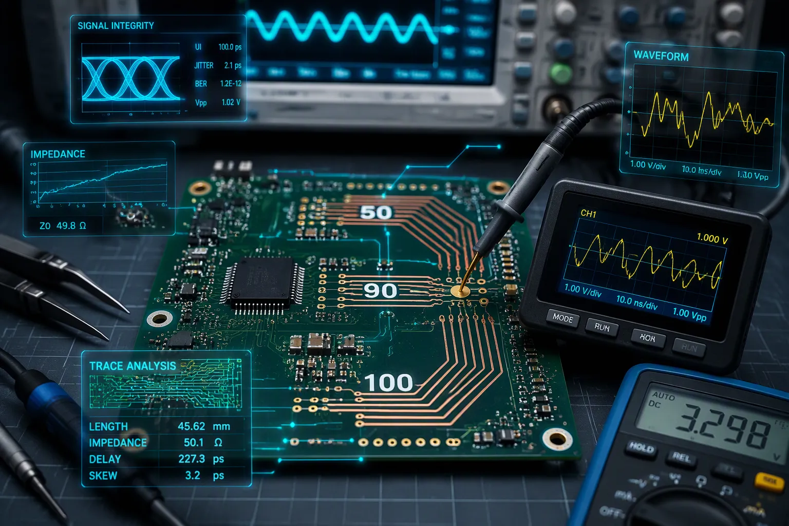
50 ohms is the compromise among signal loss, power handling, and voltage capability for single-ended traces, while 90 and 100 ohms are industry-standard differential impedance targets for USB, Ethernet, HDMI, and SATA specifications.
Why Do Most PCB Use 50 ohms, and why do 90 and 100 ohms keep appearing in stackup drawings, connector datasheets, and impedance test reports?
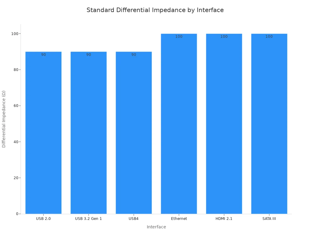
The reasons sit in engineering trade-offs, interface standards, and the consequences of using anything else. Targeting 50, 90, and 100 ohms keeps your design aligned with manufacturing and test equipment. Non-standard values create reflections, EMI, and data errors. FR-4 supports both families for most pcbs.
Key Takeaways
50 ohms balances signal loss, power handling, and voltage tolerance for single-ended traces.
90 and 100 ohms are standard differential impedances for USB, Ethernet, HDMI, and SATA.
Standard impedances match cables, connectors, and test equipment, preventing reflections and errors.
FR-4 supports 50, 90, and 100 ohms with common trace geometries and materials.
Non-standard impedances cause signal reflections, EMI, data errors, and certification failures.
Set impedance targets early in the design to avoid costly rework and ensure manufacturability.
Work with your fabricator to achieve the right tolerance, typically ±10% or tighter for high-speed interfaces.
Validate impedance with simulation and test coupons to confirm performance before production.
Why Do Most PCB Use 50 Ohms?
The 50 Ohm Compromise
Minimum Loss vs Maximum Power
No single impedance value wins every design contest. Engineers discovered this fact early in the history of radio and high-speed computing. They needed one value that worked well enough for both power delivery and signal quality. That value turned out to be 50 ohms.
The physics behind this choice is straightforward. A coaxial cable reaches minimum signal loss near 77 ohms. The same cable handles maximum power near 30 ohms. Maximum voltage tolerance sits near 60 ohms. You cannot optimize all three goals at once. You must pick a middle ground.
Design Goal | Ideal Impedance | Trade-off |
|---|---|---|
Minimum signal loss | ~77 ohms | Best for long-distance communication such as microwave links |
Maximum power handling | ~30 ohms | Used in high-power transmitters, but prone to voltage breakdown |
Maximum voltage tolerance | ~60 ohms | Resists arcing, but has higher signal loss |
Practical compromise | 50 ohms | Acceptable performance across all three categories; became standard for RF systems |
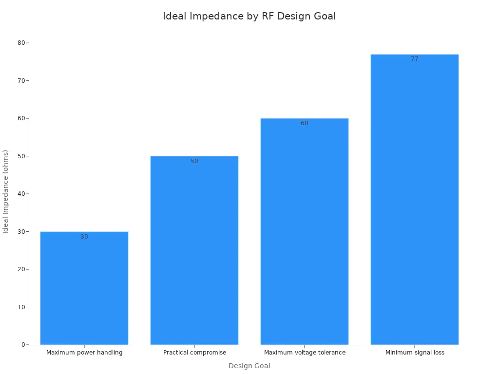
This table explains why do most PCB use 50 ohms as the default. The value sits between the loss-optimal and power-optimal points. It sacrifices a small amount of efficiency in each category to gain acceptable performance in all of them.
Voltage and Power Handling
Voltage breakdown and power transfer pull the ideal impedance in opposite directions. Lower impedance values carry more current for a given power level. That current heats the conductor and stresses the dielectric. Higher impedance values reduce current but raise the voltage stress across the insulator. A 50 ohm transmission line balances these competing risks. The compromise keeps arcing risk manageable while preserving reasonable power throughput.
You find 50 ohms everywhere because of its long history in electronics. Early radio and high-speed computer engineers needed a value that worked for both power and signal quality. They found that 50 ohms was a good compromise. Over time, test equipment, cables, and connectors all started using 50 ohms as a reference.
Why 50 Ohms Works on FR-4
FR-4 laminate makes 50 ohms easy to manufacture. You can hit this target with ordinary trace geometries and standard copper weights. A 1 oz copper trace on FR-4 with a dielectric constant of 4.5 and a 50 mil dielectric thickness requires a 13 mil trace width to achieve a single-ended 50-ohm impedance.
Parameter | Value for 50-Ohm Microstrip on FR-4 |
|---|---|
Dielectric Constant (Dk) | 4.5 |
Trace Width | 13 mils (0.33 mm) |
Dielectric Thickness | 50 mils (1.27 mm) |
Copper Thickness | 1 oz (35 μm) |
These dimensions fit comfortably inside normal fabrication tolerances. You do not need exotic materials or extreme aspect ratios. That manufacturability is a major reason why do most PCB use 50 ohms for single-ended pcb traces. The target works with the materials you already buy.
Cables and Test Equipment at 50 Ohms
Early coaxial cable designs, such as RG-58, adopted 50-ohm impedance to reduce loss and improve power transfer. As pcbs became integrated with these coaxial cables, 50 ohms became the default impedance to prevent mismatches at connectors. Over time, nearly all common RF connectors, including SMA, N-type, and BNC, were rated for 50 ohms. This history reinforced 50 ohms as the standard for coaxial cables and RF test equipment.
50 ohms has been the impedance of choice for high-speed computing since the outset of ECL and GaAs logic.
It is a useful impedance because it matches the impedance of virtually all test equipment, making accurate measurements easy.
All test equipment available for making measurements is designed with input and output impedances of 50 Ohms, and their connecting cables are also 50 Ohms, which makes 50 Ohms a good target impedance.
Pairing a 50-ohm trace with a 50-ohm connector and cable keeps signal reflection below 1%. That low reflection figure matters for measurement accuracy. Spectrum analyzers, oscilloscopes, and signal generators all present 50-ohm inputs and outputs. Your 50 ohm lines therefore connect to the bench without adapters or matching networks.
This compatibility explains why do most PCB use 50 ohms across so many product families. A 50 ohm single-ended transmission line matches the test ecosystem directly. You can probe a 50 ohm transmission line and trust the reading. The same logic applies to 50 ohm transmission lines inside instruments and 50-ohm traces on evaluation boards. Designers of 50, 90, and 100 ohms systems all benefit from this shared reference. The 50 ohm standard removes guesswork from the lab.
Why 90 and 100 Ohms Are Differential Standards
How Differential Impedance Is Defined
Differential impedance describes the impedance between two traces that carry equal and opposite signals. You place two traces close together, and their capacitive and inductive coupling shapes the impedance of the pair. The impedance of a single trace alone differs from that of the coupled pair. Trace geometry — width, spacing, and height above the ground plane — determines the final value. Increasing the spacing weakens coupling and changes the impedance.
When you control differential impedance properly, the electromagnetic fields from each trace cancel out. This cancellation reduces external interference and crosstalk. If the differential impedance is not balanced or matched, the fields do not cancel properly, and you get added noise and weakened signals. Maintaining consistent impedance along the entire trace is critical. Any change in impedance causes reflections and signal loss.
Differential Impedance | Equivalent Single-Ended Impedance | Notes |
|---|---|---|
85 Ohm | Two 42.5 Ohm lines | Routing as two 50 Ohm lines is acceptable and preferred |
95 Ohm | Two 47.5 Ohm lines | USB standard with ±15% tolerance; 50 Ohm satisfies the standard |
100 Ohm | Two 50 Ohm lines | Achieved by using two 50 Ohm single-ended transmission lines |
A 100 ohm differential impedance often comes from routing two 50 ohm single-ended lines. Tight coupling is not always necessary and can introduce drawbacks such as reduced impedance when traces sit close together. That reduction forces narrower traces and increases copper loss. Many high-speed designs follow a "not closer than" rule to avoid unwanted interaction between the two members of the pair.
USB and the 90 Ohm Standard
USB specifications require a differential impedance of 90 ohms for high-speed data pairs. This value matches the USB cable and connector requirements. When your pcb traces maintain the same impedance as the cable and connector, you prevent signal reflections and ensure reliable data transfer. The 90 ohm target balances noise protection, signal quality, and speed.
USB Standard | Data Rate | Differential Impedance Tolerance |
|---|---|---|
USB 2.0 | 480 Mbps | 90Ω ±15Ω |
USB 3.2 Gen 1 | 5 Gbps | 90Ω ±7Ω |
USB4 | 40 Gbps | 90Ω ±5Ω |
USB cables are specified at 90 Ω ±7 Ω, and connectors at 90 Ω ±15 Ω. Newer USB versions tighten the tolerance considerably. USB4 demands ±5% to meet bit error rate requirements. For most designs, ±10% is acceptable. You should always check the specific USB specification for your target data rate.
Ethernet, HDMI, and SATA: 100 Ohms
Ethernet, HDMI, and SATA all specify a 100 ohm differential impedance for their controlled differential pairs. This value matches IEEE standards for cables and PCB traces across 10BASE-T, 100BASE-TX, and 1000BASE-T networks. The 100 ohms requirement keeps network and video signals from degrading or mixing. It also matches cables and connectors to prevent signal bounce-back.
Interface | Data Rate | Differential Impedance | Tolerance |
|---|---|---|---|
Ethernet | 10–100 Gbps | 100 Ω | ±15 Ω |
HDMI 2.1 | 48 Gbps | 100 Ω | ±10 Ω |
SATA III | 6 Gbps | 100 Ω | ±20 Ω |
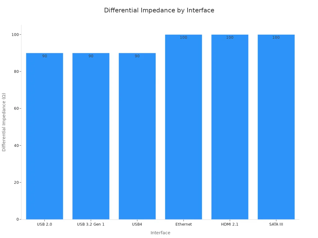
The 90 and 100 ohms values are not arbitrary. USB, Ethernet, HDMI, and SATA specifications dictate them to preserve signal integrity. A 50 ohms single-ended line is optimized for RF transmission, not for differential signaling. That is why you do not use 50 ohms for high-speed differential interfaces. The 100 ohm differential impedance standard ensures your pcbs work with the cables and connectors your customers already use.
What Actually Determines PCB Impedance
Every controlled impedance line starts with physical variables you control directly. Trace width, copper thickness, dielectric constant, layer thickness, and solder mask thickness set your pcb impedance.
Trace Width, Spacing, and Copper Thickness
Trace impedance depends first on geometry. Wider traces add capacitance to the return path, which lowers the value. Narrower traces reduce capacitance and raise it. Copper thickness works the same way: thicker copper lowers the value, while thinner copper raises it.
For differential pairs, spacing between the two traces adds another variable. Tighter spacing increases capacitive coupling and lowers differential impedance. Looser spacing reduces coupling and raises it. A 90 Ω USB pair often uses 8 mil traces with 6 mil spacing. A 100 Ω Ethernet pair can use 10 mil traces with 8 mil spacing. Both examples assume 1 oz copper on FR-4.
Your pcb trace impedance is a manufacturable result. Provide the dimensions to your fab, and the fab controls them within tolerance. Set your target values before release.
Dielectric Constant and Layer Stackup
The material between the trace and its ground plane also defines the transmission line. Dielectric constant (Dk) controls how much the signal slows and how much energy the material absorbs. Higher Dk demands a narrower trace to hold the same impedance. Lower Dk allows faster propagation with less loss.
Designing a pcb stackup means selecting material, layer thickness, and copper weight together. A 50 ohm transmission line on FR-4 uses a 13 mil trace, a 50 mil dielectric thickness, and Dk near 4.5. Those dimensions fit normal fabrication limits. Higher-speed boards use stable-Dk materials such as Rogers materials, because FR-4's Dk drifts with frequency and humidity.
Your stackup choice determines your achievable range. Change a layer distance later, and all calculated widths become invalid.
Component Matching and Reference Planes
A trace does not act alone. The return path under it sets part of the final value. A solid ground plane provides a stable return path and reduces EMI. Increase the distance between trace and plane, and the value rises. Decrease it, and the value falls.
Every discontinuity matters. Connectors, vias, and component pads add capacitance or inductance. These small changes produce reflections when they mismatch the line. Matching source and load values to the trace prevents those reflections.
When an interface specifies a 100 ohm differential impedance, pair the layout with a connector and cable rated the same. The entire chain must agree. A 50 ohm single-ended signal follows the same logic. Cables and instruments form 50 ohm transmission lines, so your traces need to match that value. Maintaining 50-ohm traces across a board keeps measurements reliable and signals clean.
Impedance control is a system-level task. You cannot adjust trace width without checking the layer stack, the return plane, and the component footprint. All variables combine into the final value.
What Happens If You Use Non-Standard Impedance
Signal Reflections and Mismatch
A non-standard trace value breaks the agreement between your pcb and everything connected to it. Signals bounce back at every impedance discontinuity and mix with the original waveform. This mixing changes the signal shape and corrupts digital data.
The damage scales with speed. At 10 Gbps, a 10% mismatch (50 ohms versus 55 ohms) can increase the bit error rate by 10x, making a high-speed link unusable. Ringing turns a logic 1 into a 0. Overshoot and undershoot push voltage spikes beyond nominal levels and can damage sensitive components such as FPGAs. Timing jitter reduces your achievable data rate. High-speed signals above 50 MHz are very sensitive to these reflection problems.
Signals bounce back and cause reflections and noise when traces do not match components, cables, and connectors
Data errors, signal loss, or electromagnetic interference can result from mismatched impedance
Connectors for fast signals are made to match certain impedance values, so always check their specs
EMI, Crosstalk, and Data Errors
Reflected signals act as tiny antennas. They radiate energy that interferes with nearby circuits, such as a 5G module disrupting GPS reception. Your board then fails FCC or CE emissions tests and may violate automotive standards like CISPR 25. EMI becomes a major problem when impedance values are uncontrolled.
Mismatch also degrades crosstalk control. Proper differential impedance keeps coupling between traces low. A wrong value weakens that control and worsens signal coupling. Elevated bit error rates follow from the combined effects of reflections, ringing, and jitter. Non-standard values also weaken signals as they travel along traces, leaving data blurry or missing at the receiver.
Interoperability and Certification Failures
Non-standard values force you into custom components. Most oscilloscopes and signal generators present 50-ohm inputs, so a mismatched trace cannot connect to the bench without adapters. Custom parts raise costs by 20 to 50%, and specialized connectors may require 12 or more weeks of lead time.
A real case shows the cost. One design used 90-ohm differential traces instead of 100 ohms. The result was 10% packet loss at 1 Gbps, eight weeks added to the timeline, a $15 per unit BOM increase, and a failed IEEE 802.3 compliance test that forced a recall. Short discontinuities sometimes prove harmless, as one reference notes about 72 to 75 ohm lines: "Rarely will this short discontinuity result in a significant degradation of the signal." Long controlled-impedance runs offer no such mercy.
Designing for 50, 90, and 100 Ohms
Set Impedance Targets Early
You should lock your impedance targets into the stackup before you route a single trace. Decide which nets need 50 ohms, which pairs need 90 ohms, and which pairs need 100 ohms. Then hand those numbers to your fabricator as part of the fabrication drawing.
This order matters. Trace width, dielectric thickness, and copper weight all depend on the target. If you change the target after layout, every calculated width becomes invalid. You must reroute the affected nets and rebuild the pcb stackup. Designing a pcb stackup around fixed targets costs far less time than fixing a finished layout.
Work with Fabricator Tolerances
Most PCB shops achieve an impedance control tolerance of ±10%. Premium manufacturers offer ±5% for critical designs. Etching tolerances directly affect the ability to hold impedance within the target window, and material Dk can vary by ±0.2. Request batch-specific Dk test data and a pre-production stackup report to confirm dielectric thickness and copper weight.
Aspect | Detail |
|---|---|
Typical impedance control tolerance | Most PCB shops achieve ±10% |
High-end impedance control tolerance | Premium manufacturers offer ±5% for critical designs |
Etch variation effect | Etching tolerances directly impact the ability to hold impedance within the target window |
Dielectric thickness / material variation effect | Material Dk can vary by ±0.2; request batch-specific Dk test data and a pre-production stackup report |
Discuss these limits with your fabricator before release. Ask which tolerance the shop can hold on your chosen stackup. A ±10% window suits most 50 ohms and 100 ohms nets. Tight interfaces such as USB4 need the tighter ±5% window.
Validate with Simulation and Test Coupons
Run a field solver on your stackup before you release the design. The simulation predicts trace impedance from width, spacing, and dielectric height. Compare the result against your target and adjust the geometry until the numbers agree.
Add impedance test coupons to the panel. The fabricator measures these coupons with a time-domain reflectometer and reports the results. This step confirms that controlled impedance in pcb design matches your simulation. Characteristic impedance in most PCB designs falls between 50 and 100 ohms, so these targets fit normal manufacturing ranges. A 50-ohm target, a 90-ohm USB pair, and a 100 ohm differential impedance all sit inside standard fabrication capability.
Why Standard Values Simplify PCB Design
Simpler Stackup and Manufacturing
Standard impedance values remove guesswork from your stackup planning. PCB manufacturers already maintain qualified materials and stackups for 50 ohm boards. You reuse proven processes instead of requesting custom layer arrangements. Standard 50 ohm trace widths fit most fabrication shops, so you avoid extra manufacturing iterations. FR-4 and standard board thicknesses keep material costs low and improve yield.
Best practices for controlled impedance designs, such as symmetrical stackups and dedicated ground planes, are well established. You encounter fewer production and testing surprises. Standard 50, 90, and 100 ohm values work with off-the-shelf cables, connectors, and test equipment. Non-standard values force custom components. Custom 60 ohm coaxial cables can increase cost by 20 to 50 percent, and specialized connectors can require 12 or more weeks of lead time.
Impedance | Primary Practical Benefit | Manufacturing Advantage |
|---|---|---|
50 ohms | Balances power handling, signal loss, and voltage tolerance | Matches standard coaxial cables and test gear; easily achieved on FR-4 |
90 ohms | Minimizes crosstalk and reflections in differential pairs | Aligns with standard USB cable impedance; fabricable on FR-4 |
100 ohms | Optimizes noise immunity for differential signaling | Matches standardized cables and connectors; reduces custom component costs |
Easier Testing and Troubleshooting
Most oscilloscopes and signal generators have 50 ohm inputs. Your standard PCB designs connect directly to this equipment without adapters. You measure impedance accurately and avoid test-fixture iteration. Time Domain Reflectometry measures reflections to calculate impedance along the trace. Vector Network Analyzers test impedance across frequency for RF designs. Signal integrity simulations predict eye diagrams and bit error rates.
The 50 ohm single-ended standard emerged from coaxial cable design. Maintaining 50 ohms on PCB traces ensures minimal signal reflection, typically under 1 percent. This low reflection preserves signal integrity in systems like 5G and radar. Differential signaling uses two complementary traces to reduce noise and crosstalk. The 90 ohm standard for USB balances data rate, cable compatibility, and manufacturability on standard FR-4 PCBs. The 100 ohm standard for Ethernet supports long-distance transmission by reducing crosstalk in multi-pair cables.
Q: Why do USB and Ethernet use different differential impedances? A: USB prioritizes compactness, favoring 90 ohms. Ethernet focuses on long-distance transmission, where 100 ohms reduces crosstalk in multi-pair cables. These values are locked to their respective standards to ensure interoperability.
Cross-Vendor Compatibility
Standard impedance values improve compatibility across chips, connectors, cables, and test equipment. Coaxial cables such as RG-58 and connectors such as SMA, N-type, and BNC are standardized at 50 ohms. Matching PCB traces avoids impedance mismatches at every interconnect. The USB standard specifies 90 ohms differential impedance for both PCB traces and USB cables. This enables chip-to-cable compatibility with minimal reflections and crosstalk.
High-speed chips are designed around standard I/O impedances. Non-standard traces cause reflections that can corrupt data and damage sensitive components such as FPGAs. Off-the-shelf cables, connectors, and probes are manufactured for 50, 90, or 100 ohms. You avoid the cost and lead time of custom non-standard components. Standard values reduce design complexity, lower manufacturing cost, ensure signal integrity, and avoid EMI or regulatory failures.
You now know why do most pcb use 50, 90, and 100 ohms for impedance. The 50 ohms target solves the single-ended trade-off among loss, power, and voltage. The 90 and 100 ohms values serve the differential signaling standards for USB, Ethernet, HDMI, and SATA. Standard values remove guesswork from stackup planning, fabrication, connector selection, and signal integrity testing. High-speed pcb design is not about inventing new impedance values. It is about following proven standards. Target 50, 90, or 100 ohms unless a specific chip vendor or interface specification explicitly requires a different value.
FAQ
Why does 50 ohms dominate single-ended PCB traces?
Engineers needed one value that balanced signal loss, power handling, and voltage tolerance. The loss-optimal point sits near 77 ohms, while maximum power transfer occurs near 30 ohms. The 50-ohm compromise also matches coaxial cables like RG-58 and nearly all RF test equipment, so your traces connect directly to the bench.
Can I use 50 ohms for USB or Ethernet differential pairs?
No. USB specifications require 90 ohms differential impedance, and Ethernet, HDMI, and SATA specify 100 ohms. These values match the cables and connectors your customers already use. A 50-ohm single-ended line is optimized for RF transmission, not differential signaling, so mismatches would cause reflections and data errors.
How tight should my impedance tolerance be?
Most PCB shops hold ±10% impedance control. Premium manufacturers offer ±5% for critical designs. USB4 demands ±5% to meet bit error rate requirements, while USB 2.0 allows ±15%. Always check your target interface specification and confirm the achievable tolerance with your fabricator before release.
What happens if my trace impedance drifts from the target?
Signals bounce back at every impedance discontinuity and mix with the original waveform. At 10 Gbps, a 10% mismatch can increase bit error rate by 10x. Reflected signals also radiate energy that interferes with nearby circuits, causing you to fail FCC or CE emissions tests.
Does FR-4 support 50, 90, and 100 ohms?
Yes. A 50-ohm microstrip on FR-4 with a dielectric constant of 4.5 and 50 mil dielectric thickness needs a 13 mil trace width. A 90-ohm USB pair often uses 8 mil traces with 6 mil spacing. A 100-ohm Ethernet pair can use 10 mil traces with 8 mil spacing. All fit standard fabrication tolerances.
Why do USB and Ethernet use different differential impedances?
USB prioritizes compactness, favoring 90 ohms. Ethernet focuses on long-distance transmission, where 100 ohms reduces crosstalk in multi-pair cables. Each value is locked to its respective standard to ensure interoperability across chips, cables, and connectors.
How do I verify my impedance after fabrication?
Add impedance test coupons to the panel. Your fabricator measures these coupons with a time-domain reflectometer and reports the results. This step confirms that controlled impedance in your PCB design matches your simulation. Run a field solver on your stackup before release to predict trace impedance from width, spacing, and dielectric height.
What is the most common mistake in impedance design?
Changing impedance targets after layout. Trace width, dielectric thickness, and copper weight all depend on the target. If you change the target after routing, every calculated width becomes invalid. You must reroute the affected nets and rebuild the stackup. Lock your targets into the stackup before you route a single trace.
