Essential PCB Design Terms Every Engineer Should Know
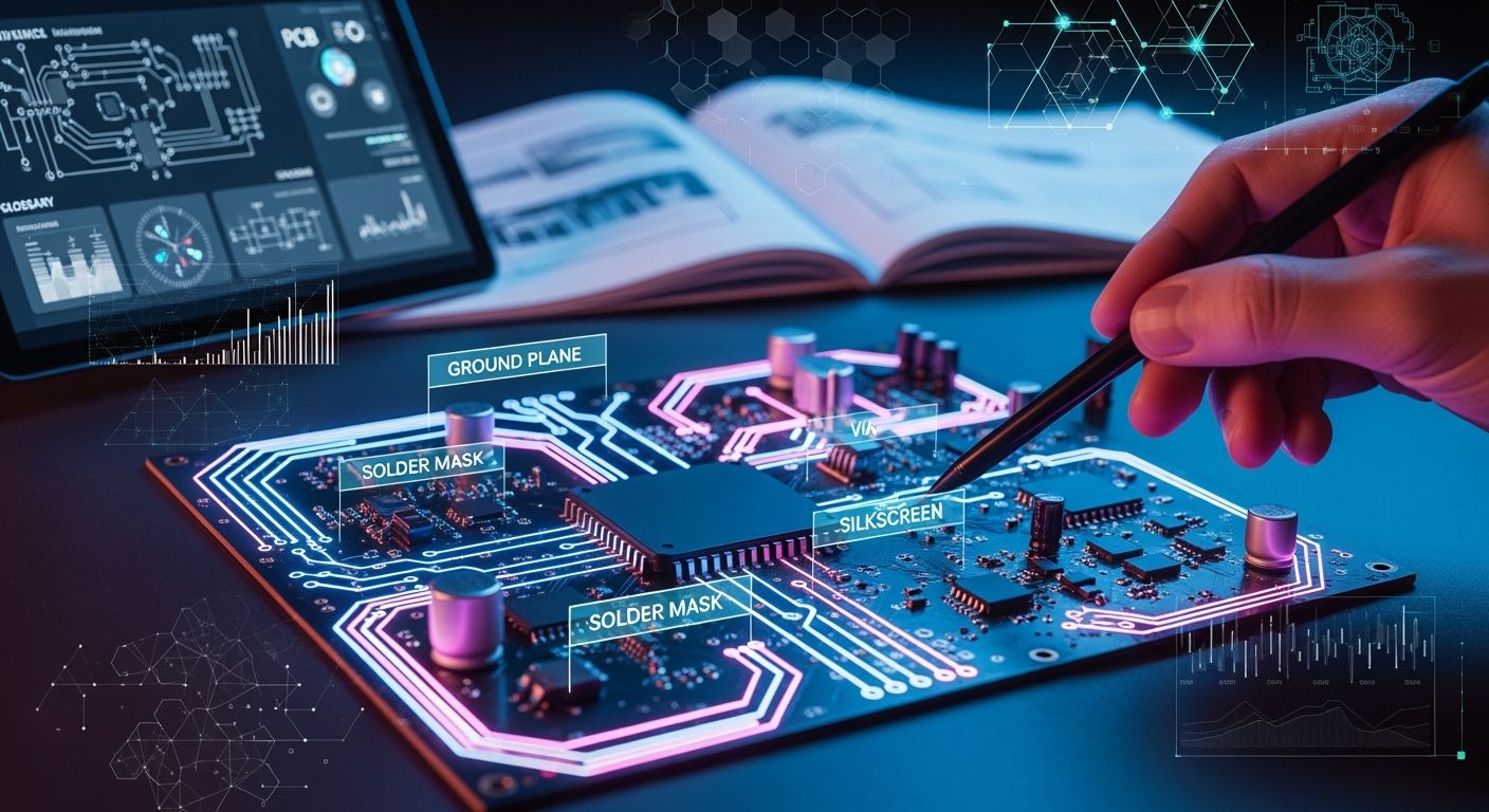
You must know PCB Design Terms to work well with others. This helps you make good products. When you know these words, you can read hard papers easily. You can also talk with manufacturers and stop costly mistakes. Use this guide if you need to remember or check a word. It will help you with your work every day.
Key Takeaways
Knowing PCB design words helps you talk clearly with your team and people who make the boards. A schematic is like a map for your circuit. It lets you find and fix mistakes before you build it. Picking the right pad size makes solder joints strong. It also stops parts from moving or not lining up. Good stackup planning keeps signals clear. It can stop data mistakes in your circuit. Checking Gerber files before sending them in helps you avoid expensive errors when making PCBs.
Essential PCB Design Terms
Schematic
A schematic is like a map for your circuit. It shows how parts connect together. This map helps you not make mistakes. You can check if your circuit works before building the printed circuit board. If you know how to read schematic diagrams, you can find errors early. You can also fix problems fast. This step is important in pcb design terms because it leads the whole process.
Netlist
A netlist is a list that shows how parts connect in your circuit. You use this list to go from schematic to pcb layout.
Netlists help keep your circuit connections right from start to end.
They let you use pcb design tools to draw traces and make Gerber files for building.
Netlists help your circuit stay strong as you work through each design step.
Trace
A trace is a thin copper line on your pcb. It moves signals or power between parts.
For fast circuits, you use 50Ω traces for single signals and 100Ω for pairs.
Traces need the right width to keep signals clear and strong.
You should know this basic pcb terminology to stop signal loss and mistakes.
Pad
A pad is a flat copper spot where you put and solder a part. Pad size and shape are important for soldering and placing parts.
Tip:
If you pick the right pad size, you get good solder flow and strong joins. Pads that are too big can make parts float or connect by mistake. Pads that are not the same size can make parts stand up instead of lying flat.
Pad Size Considerations | Implications |
|---|---|
Proper pad dimensions | Good solder flow, fewer defects |
Pad size matches lead sizes | Accurate placement, strong connections |
Oversized pads | Floating parts, solder bridging |
Unequal pad sizes | Tombstoning in two-terminal components |
Via
A via is a hole that links layers in your pcb. You use different vias for different jobs.
Through-hole via links top and bottom layers.
Blind via joins outer layers to inside layers.
Buried via links only inside layers.
Microvia is tiny and used in crowded designs.
Via-in-pad sits in a pad for tight spaces.
Filled, tented, capped, stacked, and backdrilled vias make your board stronger and signals better.
Annular Ring
The annular ring is the copper around a drilled hole. You find its width by taking the pad size, subtracting the hole size, and dividing by two.
This ring is needed for strong electrical joins. If the ring is too small, you might get open circuits or weak spots. A good annular ring keeps your printed circuit board working well.
Stackup
Stackup is how you put layers in your pcb. Each layer can carry signals, power, or be a ground.
Stackup changes how your board handles noise and other signals.
A 4-layer stackup keeps fields tight and loops small.
A 6-layer stackup gives more shielding and balanced power.
An 8-layer stackup keeps signals apart for mixed circuits.
Top signal/component layer
First inside ground plane
Inside power plane
Inside signal layer
Second inside ground plane
Bottom signal/component layer
Stackup choices help your device work well and avoid electromagnetic problems.
Impedance
Impedance is how much your pcb traces slow down electricity. You control impedance by changing trace width, space, and stackup.
If impedance is wrong, signals bounce back and cause errors.
Crosstalk can happen between traces and mess up data.
Good impedance keeps your circuit signals clear and strong.
Plane
A plane is a big copper area in your pcb. You use planes for power or ground.
Power planes spread current well and keep voltage steady.
They cut down noise and heat, so your circuit stays safe.
Planes give signals a low-impedance path and stop interference.
Silk Screen
Silk screen is the printed words and symbols on your pcb. It shows where parts go and which way they face.
Silk screen helps you put parts in the right spot and fix problems.
Machines print silk screen for speed and accuracy.
Solder Mask
Solder mask is a cover that goes over your pcb. It keeps copper traces safe and stops solder from joining them by mistake.
Solder mask stops short circuits and keeps your board safe from water and dust.
It only leaves open the spots you need to solder, so building is easier.
Surface Finish
Surface finish is a layer on top of copper pads. It keeps them safe and helps with soldering.
HASL is cheap and easy but not good for tiny parts.
ENIG uses nickel and gold for good soldering and stops rust.
ENEPIG adds palladium for more strength.
Immersion silver is good for fast circuits but needs careful storage.
Copper Weight
Copper weight is how thick the copper is on your pcb.
More copper lets you move more current and spread heat better.
1oz copper is good for low power but gets hot with high current.
2oz copper cuts heat in half and keeps things cooler.
Copper weight, trace width, and thermal vias all help your printed circuit board handle power and heat.
HDI (High-Density Interconnect)
HDI lets you fit more parts and traces in a small space.
You use blind and buried vias to save space and stop crowding.
HDI helps you make smaller things like phones and medical tools.
It makes signal paths better and keeps your circuit strong.
DFM (Design for Manufacturability)
DFM means you design your pcb so builders can make it easily and with no mistakes.
Manufacturers’ benefits | Designers’ benefits |
|---|---|
Fits their process, avoids yield issues | Matches features to capabilities, finds errors early, reduces delays |
DFM helps you not waste money on fixes and keeps talking clear with the fab house. You get better boards and fewer mistakes.
Note:
Many engineers mix up pcb design terms. Look at this table to see common mistakes:
Misunderstood Term | Explanation |
|---|---|
Blind vs Buried Vias | Blind vias join outer layers to inside layers; buried vias join only inside layers. |
Pad vs Land | These words mean the same part but are used in different ways. |
Solder Mask vs Silkscreen | Solder mask is a cover, while silkscreen is printed text. |
Trace vs Track | 'Trace' is American, 'track' is British for the same thing. |
Through-Hole Context | Means either a part with leads or a hole that goes through the board. You need to know the context. |
You need to know pcb design terms and basic pcb terminology to not make mistakes and build good printed circuit boards.
Printed Circuit Board Manufacturing Terms
Gerber Files
You need Gerber files to begin making a pcb. These files are like a common language for your cad design and the factory. Gerber files have all the details for your printed circuit board. They include copper layers, silk screen, solder mask, and drill data. When you send these files, the pcb fabrication team knows your design. Using standard formats helps stop mistakes and keeps your circuit right.
Tip: Always look over your Gerber files before sending them to stop expensive errors.
Aspect | Explanation |
|---|---|
Universal Language | Gerber files help you and builders understand each other. |
Detailed Information | They show all parts of your pcb layout and where parts go. |
Standardization | Standard formats keep your details clear and easy to follow. |
Panelization
Panelization lets you put many pcbs on one big board when making them. This step makes building faster and costs less money. You can fit your circuit designs into normal panel sizes, which saves materials. Batch processing means you get more printed circuit boards at the same time. After making them, you split each pcb using scoring or tab routing. This keeps your boards strong and neat.
Panelization helps make more pcbs at once.
It cuts down waste and saves money.
Clean ways to split boards keep your circuit edges safe.
PCB Stackup
PCB stackup is the order and number of layers in your printed circuit board. You must plan your stackup in your cad design to meet all the rules. More layers can make pcb fabrication harder and cost more money. Features like buried or stacked vias need careful planning and extra steps. These choices change how well your circuit works and how much you pay.
More layers make things harder and cost more.
Special vias need careful planning in your cad files.
Stackup changes signal quality and how well your board works.
FR-4
FR-4 is the most used material for pcb manufacturing. It is a flame-proof fiberglass-epoxy laminate. You pick FR-4 because it gives good electrical insulation, strong support, and can take heat. These things make it great for most circuit jobs. FR-4 keeps your pcb safe and steady, even in tough places.
FR-4 does not burn easily and stands up to heat.
It gives your circuit strength and lasts a long time.
It works for many needs in pcb fabrication.
Drill Hit
Drill hit is the exact spot where a drill makes a hole in your pcb. Good drill hits are needed for strong plated through holes. If the drill misses, your circuit can lose connection or get weak. Good drilling keeps your details right and your pcb strong.
Note: Dust, dirt, or broken drill bits can mess up drill hits and cause problems in your printed circuit board.
Feature | Tolerance |
|---|---|
Drill for PTH | ±3 mils |
Drill for NPTH | ±2 mils |
Via location | 1 mil |
You must check drill hits in your cad files to match all the rules and stop problems when making your pcb.
PCB Assembly and Testing Terms
BOM (Bill of Materials)
You need a BOM to start pcb assembly. This list shows every circuit part you must buy and use. The BOM helps you get the right parts at the right time. You avoid delays and keep your printed circuit board project on track.
The BOM makes sourcing easy by listing all materials.
You control details and make sure every part fits your design.
Good BOM management helps you reach higher first-pass yield and reduces errors.
You save time and resources by avoiding rework.
Pick and Place
Pick and place machines move parts onto your pcb fast and with high accuracy. You use these machines for complex circuit layouts.
They boost productivity and let you build dense designs.
Automation cuts errors and lowers labor costs.
You place tiny parts like microprocessors and SMDs with ease.
Rapid and precise operations streamline component placement.
Less production time means more boards finished.
Fewer mistakes and less waste save money.
Pick and place machines changed pcb assembly. You can handle tiny parts and complex layouts, which increases throughput.
SMT (Surface Mount Technology)
SMT lets you place parts directly on the pcb surface. You use SMT for fast circuit builds and high-density designs.
SMT speeds reach 50,000–90,000 placements per hour.
You get precision of ±15 μm, which is key for fine-pitch parts.
SMT fits hundreds of parts, including BGAs and tiny passives.
THT (Through-Hole Technology)
THT uses holes in the pcb for part leads. You solder these leads for strong joins.
THT works well for parts that need extra strength.
You use THT for connectors and big circuit parts.
THT is slower than SMT but gives solid connections.
Reflow Soldering
Reflow soldering melts solder paste to join parts to the pcb. You use this method for SMT parts.
The process heats the board in stages.
You get reliable joins and fewer defects.
Reflow works best for high-speed circuit builds.
AOI (Automated Optical Inspection)
AOI checks your pcb assembly for errors. You use AOI after reflow soldering.
AOI finds bad solder joints and misplaced parts.
It helps you keep quality high and avoid defects.
AOI uses cameras and software to inspect every circuit.
ICT (In-Circuit Test)
ICT tests your pcb for electrical problems. You use ICT to check if every circuit works.
ICT finds shorts, opens, and wrong parts.
You get fast feedback and fix issues early.
ICT helps you meet design for manufacturing goals.
Flying Probe Test
Flying probe test uses moving probes to check your pcb. You use this test for small batches or new designs.
It finds faults without needing custom fixtures.
You test every circuit path and part.
Flying probe is flexible and works for prototypes.
Quality control in pcb assembly uses many tools. You rely on functional testing, solder paste inspection, AOI, and statistical process control to keep your boards reliable. Closed-loop feedback lets you fix problems before they grow.
Testing Method | Purpose |
|---|---|
Functional Testing | Checks board performance |
SPI | Finds solder paste issues |
AOI | Inspects assembly and solder joints |
SPC | Monitors process stability |
Closed-Loop Feedback | Adjusts equipment to prevent defects |
Common PCB Terminology Mistakes
Trace vs. Net
People sometimes mix up "trace" and "net." A trace is a real copper line on your PCB. It moves signals or power between parts. A net is a connection shown in your schematic. It tells you which pins should link together. Mixing these up can make you read your design files wrong. This might cause mistakes in layout or when making the board.
Tip: Always look at your schematic and layout. Make sure nets and traces match.
Solder Mask vs. Silk Screen
Solder mask and silk screen do not do the same job. Solder mask is a layer that protects copper traces. It stops solder from joining places it should not. Silk screen is printed words or pictures. It helps you know where parts go and how to place them.
Term | Function |
|---|---|
Solder Mask | Protects copper, prevents shorts |
Silk Screen | Shows labels and part outlines |
If you mix these up, you might put parts in the wrong spot. You could also risk short circuits. |
PCB Stackup Importance
Stackup is the order of layers in your PCB. You need to plan stackup to keep signals and power working right. If you forget about stackup, you can get data errors or your system may not work. High-frequency designs need good stackup to stop crosstalk and noise.
Good stackup keeps signals strong and clear.
Bad stackup can cause voltage drops and too much heat.
DFM vs. DFA
DFM means you design your board so it is easy to make. DFA means you design your board so parts are easy to put on and solder. If you do not think about these, your board may be hard to build or put together.
🛠️ Always talk to your manufacturer and assembly team before you finish your design.
Via Types Confusion
You use vias to link layers in your PCB. There are through-hole, blind, buried, and microvias. Picking the wrong via can cause problems when making your board. Some vias need special steps to make. If you forget about these, your board may not be possible to build.
Through-hole vias link all layers together.
Blind vias link outside layers to inside layers.
Buried vias link only inside layers.
Microvias fit in small spaces.
Common Mistakes in PCB Design:
Not thinking about signal integrity can cause errors.
Bad power planning can make voltage drop and cause heat.
Forgetting about heat can make parts break.
Not thinking about how to build the board makes it hard to produce.
Remember, using the right words helps you avoid mistakes and keeps your project going well.
You build better projects when you know PCB design terms. You talk clearly with your team and avoid mistakes. You keep learning as technology changes. Use this list as your daily reference.
Check terms before you start a new design.
Review definitions when you read documentation.
Share this guide with your team.
Keep this checklist handy. You stay prepared and confident in every engineering task.
FAQ
What is the difference between a schematic and a PCB layout?
A schematic shows how parts connect in your circuit. You use it to plan and check your design. A PCB layout shows where you place parts and traces on the board.
Why do you need a solder mask on your PCB?
A solder mask protects copper traces from short circuits and damage. It keeps solder from spreading to unwanted areas. This layer helps your board last longer and work better.
How do Gerber files help in PCB manufacturing?
Gerber files tell the factory exactly how to build your board. They include all the details for copper layers, holes, and markings. You must check these files before sending them to avoid mistakes.
What does DFM mean for your PCB project?
DFM stands for Design for Manufacturability. You use DFM to make sure your board is easy to build. This step helps you avoid costly errors and delays during production.
See Also
Key Skills Required for Effective Multi-Layer PCB Layout
Understanding High-Speed PCB Design and Its Importance
Comprehensive Overview of Flexible PCB Production Techniques
Defining PCB Printed Circuit Boards and Their Fundamental Principles
