PCB Solder Mask Design: Types & Basic Requirements
You use a solder mask to keep copper circuits safe on a PCB. It stops damage and keeps solder from joining parts by mistake. Solder Mask Design helps your circuit work well by blocking bad connections. It also protects important spots. There are many types of solder mask in the industry. Some types are liquid photoimageable, epoxy, dry film, and flexible formulas. Liquid photoimageable solder mask is used most. It covers over 75% of the market. When you pick and design solder mask, you must think about thickness, alignment, color, and reliability. This helps your circuit work its best.
Key Takeaways
Solder masks keep copper circuits safe on PCBs. They stop solder from connecting by accident and protect from damage.
Pick the right solder mask for your PCB design. Liquid photoimageable masks work well for crowded layouts.
Keep the solder mask thick enough to stop shorts. This helps your PCB work well. Follow IPC rules for your project.
Make sure the dam width and alignment are correct in your design. This stops solder bridges and keeps connections strong.
Choose solder mask materials that fit your board’s heat and chemical needs. This helps your PCB work its best.
Types of Solder Mask
You have different solder mask types for PCB designs. Each type works in its own way. Each has good points and best uses. Knowing about these types helps you pick the right one.
Liquid Epoxy Solder Mask
Liquid epoxy solder mask is made from resin, hardener, filler, solvent, pigment, and additives. You put it on the board with screen printing. After that, you heat the board to dry the mask. Then, you develop and cure it to make the layer strong.
Components | Common Material |
|---|---|
Resin | Epoxy or Epoxy acrylate |
Hardener/Catalyst | Aromatic or Amine |
Filler | BaSO4, SiO2 |
Solvent | Organic solvent |
Pigment | Phthalocyanine green |
Additive | Defoaming agent |
Screen printing starts the curing process. You dry the mask at 130–160°C for 15–70 minutes. After drying, you wash away parts not exposed with alkaline solution. The last cure is at 100–200°C for at least 30 minutes. This makes the mask stable in heat.
Tip: Liquid epoxy solder mask is best for simple PCB designs and making lots of boards.
You get basic protection from water and rust. This solder mask costs less and is easy to use. It does not give sharp details or strong chemical resistance. You should not use it for boards with lots of parts or harsh conditions.
Property | Epoxy-based | Acrylic-based | Urethane-based |
|---|---|---|---|
Adhesion | Excellent | Good | Very Good |
Thermal Resistance | High | Moderate | High |
Dielectric Strength | High | Moderate | High |
Chemical Resistance | Excellent | Good | Very Good |
Flexibility | Low | Excellent | Good |
Advantages:
Low cost
Good for simple boards
Works well for big batches
Limitations:
Cannot make tiny details
Not good for crowded boards
Weak against strong chemicals
Liquid Photoimageable (LPI) Solder Mask
Liquid photoimageable solder mask uses a UV-sensitive liquid. You spray or screen print it on the board. Then, you shine UV light on the board. The mask gets hard only where you want it. This gives you very accurate results.
LPI solder mask helps you make tiny features and close spaces.
You stop the mask from covering pads or vias.
You lower the chance of solder bridges and shorts.
Application Type | Benefits |
|---|---|
High-Density Interconnect (HDI) | Stops solder bridges, keeps circuits working. |
BGA Layouts | Handles complex layouts with tight spaces. |
Fine-Pitch Components | Great for designs needing high accuracy and close spaces. |
Liquid photoimageable solder mask is best for most rigid PCBs. It works well for HDI boards and tiny parts. The thin layer and UV curing are good for modern electronics.
Note: Use LPI solder mask for designs needing high accuracy and close spaces.
Dry Film Solder Mask
Dry film solder mask is a solid sheet. You stick it to the PCB with a vacuum machine. After that, you shine UV light on the board. You wash the mask in water and cure it with UV light.
Application Type | Typical Thickness Range (μm) | Typical Thickness Range (mils) | Performance Impact |
|---|---|---|---|
Standard PCBs | 20-30 | 0.8-1.2 | Gives electrical insulation, protects from the environment, and controls solder. |
High-density interconnect | 15-25 | 0.6-1.0 | Helps control impedance in high-frequency boards. |
Flex and rigid-flex PCBs | 10-20 | 0.4-0.8 | Makes the board more flexible. |
High-frequency applications | 15-25 | 0.6-1.0 | Changes impedance of transmission lines. |
Power electronics | 30-50 | 1.2-2.0 | Helps manage heat and cool the board. |
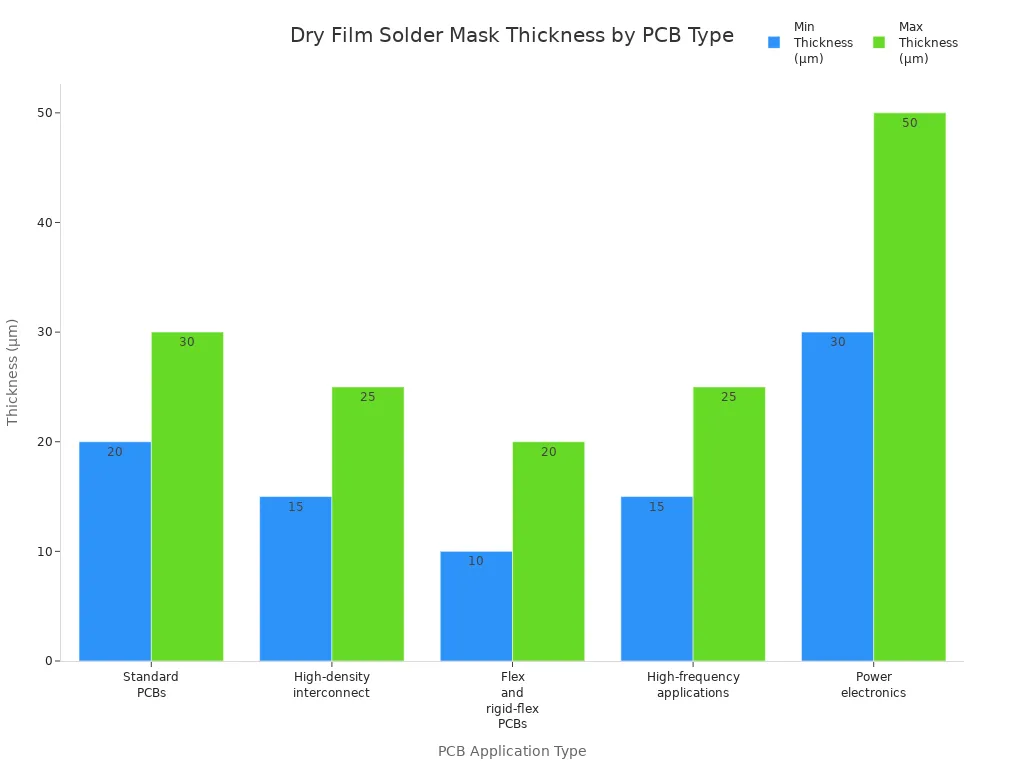
You get even thickness and strong protection. Dry film solder mask helps control impedance in high-frequency boards. It helps manage heat and makes flex PCBs bend better. You must clean the PCB, stick the film, shine UV, wash, and cure it.
Tip: Dry film solder mask is good for boards needing even thickness and high reliability.
Impedance control: Thickness changes transmission lines.
Thermal management: Helps cool the board.
Flexibility: Works for flex and rigid-flex PCBs.
Manufacturing yield: Right thickness stops defects.
Dry Film Photoimageable Solder Mask
Dry film photoimageable solder mask is a photosensitive polymer in a solid sheet. You stick it to the PCB with a vacuum. You shine UV light through a mask. The UV light hardens the parts you want to keep. You wash away soft parts and cure the mask with heat.
Criteria | Dry Film Solder Mask | LPI Solder Mask |
|---|---|---|
Application Method | Vacuum lamination | Spraying or silkscreening |
Thickness Uniformity | High (0.8-1.2 mils) | Variable (0.5-1.5 mils) |
Precision for Fine-Pitch | Excellent (down to 3 mils) | Moderate (down to 4-5 mils) |
Processing Time | Longer (1-2 hours) | Faster (under 30 minutes) |
Cost | Higher | Lower |
Best for | High-density, high-frequency designs | Standard designs, prototypes |
Dry film photoimageable solder mask gives you great accuracy and even thickness. You can use it for boards with lots of parts and high-frequency needs. It works well for making many boards. You get a strong layer that stops rust and insulates traces.
Note: Dry film photoimageable solder mask is best for tough jobs needing even layers and strong protection.
You put the film on as a solid sheet. You use vacuum, heat, and pressure to stick it to the PCB. UV light lets you make exact openings in the mask.
Now you know the main solder mask types. Each type has special benefits for different PCB designs. You can pick the best solder mask for your project.
Solder Mask Design Requirements
Solder Mask Layer Thickness
You need to control how thick the solder mask is. The right thickness keeps your PCB safe. It stops shorts and protects copper. There are rules for each reliability class. You can see these in the table below:
IPC Class | Minimum Solder Mask Thickness |
|---|---|
Class 1 (General Electronic Products) | No minimum thickness requirement |
Class 2 (Dedicated Service Electronic Products) | Minimum 10μm |
Class 3 (High-Reliability Electronic Products) | Minimum 18μm |
You must follow these rules when you design the solder mask. The solder mask layer acts like an insulator. It stops short circuits between traces and parts. It also keeps copper safe from water and chemicals. A thicker layer gives better protection from scratches and rust. But if it is too thick, it can crack when hot. You need to balance thickness for safety and strength.
The solder mask layer stops shorts and keeps signals clear.
It protects copper from rust and tough places.
Thickness changes how signals move in fast boards.
Thick layers stop scratches and chemicals.
Too much thickness can crack with heat.
Tip: Always check the IPC class for your PCB. Pick the right solder mask thickness for your board.
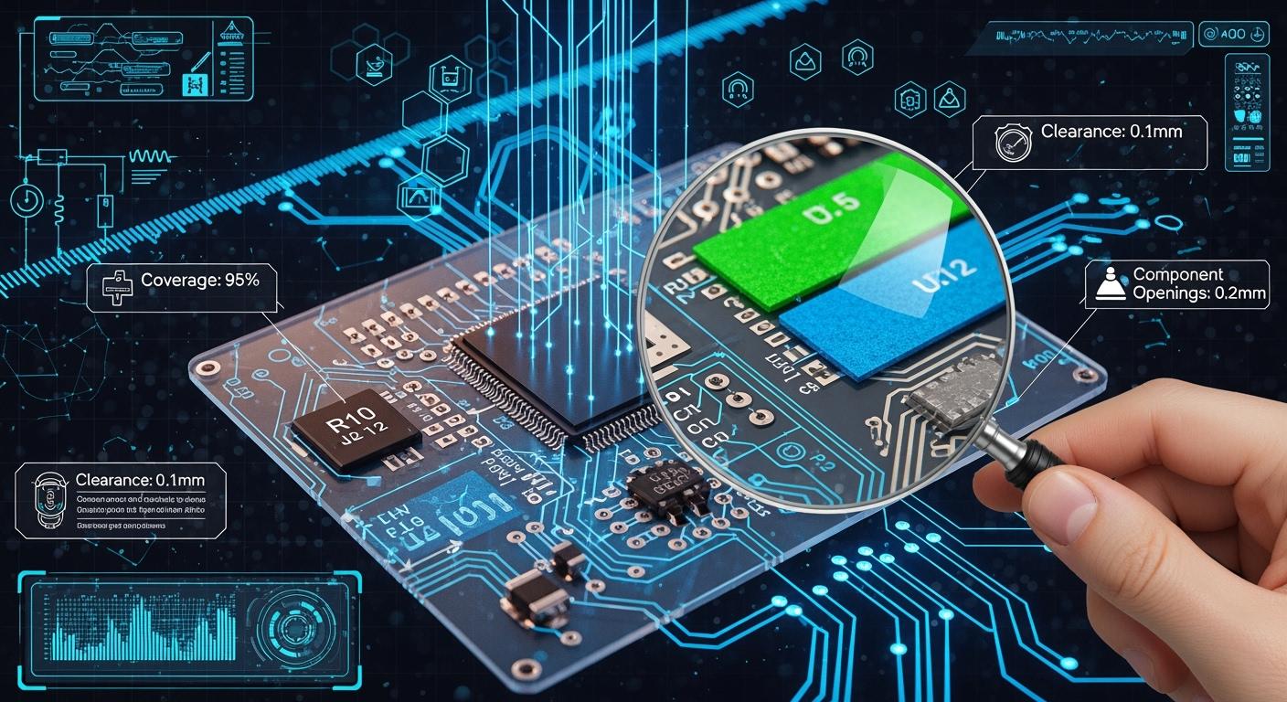
Solder Mask Dam Width & Alignment
You need to set the right dam width in your design. The dam is the space between pads. It stops solder from joining pads and making shorts. For green liquid photoimageable solder mask, use at least 0.1 mm. For black and white solder mask, use at least 0.15 mm. These sizes help stop solder bridges on busy boards.
Green LPI solder mask: Dam width at least 0.1 mm.
Black and white solder mask: Dam width at least 0.15 mm.
Good dam width stops solder bridges.
You also need to line up the solder mask with the pads. Good alignment keeps pads open for soldering. Bad alignment can make weak joints, solder balls, or open spots. If you miss the dam, solder can bridge pads. Hidden problems can cause the board to fail when hot or shaking.
Bad alignment makes pads smaller and weakens joints.
Exposed copper can cause solder balls and shorts.
Mistakes can remove the dam and cause bridges.
Solder balls that are not flat cause problems.
Hidden problems make the board less reliable over time.
Note: Always check dam width and alignment in your design. This step helps your board work better and last longer.
Color & Material Selection
You can pick from many solder mask colors. Each color changes how you check and use the board. Green is most common. It gives high contrast and is easy to inspect. Red, blue, black, white, and yellow look different and have special uses. The table below shows the main colors and what they do:
Solder Mask Color | Characteristics | Influence on Inspection and Performance |
|---|---|---|
Green | High contrast, thermal stability, chemical resistance | Best for manual and automated inspection, used in demanding applications |
Red | Moderate contrast, aesthetic differentiation | Used for visual uniqueness, moderate durability |
Blue | Matte finish, softer contrast | Helps in specific lighting for visual inspection, highlights flux/residue |
Black | Absorbs heat and light | Reduces contrast, complicates visual inspection, used for low-reflective designs |
White | Reflects heat and light | Challenges during reflow, reveals contamination, used in optical assemblies |
Yellow | Limited contrast | Complicates inspection, used for specialty prototypes, not widely adopted |
You must choose solder mask materials that fit your board’s needs. For boards that get hot, pick materials that resist chemicals, stick well, and handle heat. The mask must take soldering heat, which can go over 220°C. You need strong insulation to stop shorts. Balance flexibility and hardness for both stiff and bendy boards. Flame retardance is important for safety.
Property | Description |
|---|---|
Chemical Resistance | The mask must resist chemicals used in PCB processing like fluxes, cleaners, and etchants. |
Adhesion | Strong adhesion to the substrate ensures the mask stays intact on the board. |
Thermal Stability | The mask must withstand high temperatures during solder reflow which can exceed 220°C. |
Dielectric Strength | High dielectric strength prevents arc-overs or short circuits. |
Flexibility & Hardness | The mask needs a balance between flexibility to handle PCB flexing and hardness to abrasion. |
Flame Retardance | The mask should self-extinguish when exposed to an open flame. |
Pick solder mask materials with high glass transition temperature (Tg) for hot boards.
Tip: Green solder mask is best for checking your board. Choose materials that fit your board’s heat and chemical needs.
Reliability Classes & Standards
You must follow reliability classes and standards in your design. IPC-SM-840 sets the main classes for solder mask. Each class is for a different use:
Class | Description |
|---|---|
T | Telecommunications devices, suited for high-performance industrial and commercial products. |
H | High reliability/military applications where uninterrupted service is essential. |
FT | Flexible printed board applications in telecommunications. |
FH | Flexible printed board applications in high reliability/military contexts. |
You need to match your design to the right class. High-reliability boards use Class H or FH. Flexible boards use FT or FH. Standards like IPC-A-600K give rules for mask coverage and via treatment. These rules help you keep your board safe from the environment.
Solder mask standards help you with advanced board features. You can pick solder mask defined or non-solder mask defined pads. Non-solder mask defined pads help copper stick and carry more current. Solder mask defined pads control solder for small parts. Standards make sure your design fits tight layouts and meets tough needs.
Note: Always use the right class and follow IPC standards in your design. This step helps your board last longer and work better for both stiff and bendy boards.
Choosing Solder Mask for PCB
Design & Manufacturing Considerations
Think about your pcb design before picking a solder mask. The best solder mask depends on how crowded your board is. It also depends on where the board will be used and how it is made. High-density boards need a mask that stops solder from joining parts. Liquid photoimageable masks are good for these boards. Special masks are better if your pcb faces strong chemicals or heat.
Factor | Recommendation |
|---|---|
Application Environment | UV-resistant for outdoor, high Tg for high-temperature, epoxy for chemical |
Electrical Requirements | Low Dk/Df for high-frequency, high breakdown voltage for high-voltage |
Process Requirements | High-resolution LPI for high-density, dry film for mass production, cost evaluation for sensitive applications |
You make pcb manufacturing better by leaving space around pads and vias. Do not let mask slivers get between tiny leads. Keep dam width above the limits for making boards. Make sure mask openings match pad shapes to stop mistakes. Mask thickness changes how electricity moves and keeps the board safe. Control thickness so assembly is easy.
Tip: Always pick a solder mask that fits your pcb design and how you build it.
Application Methods
Different ways to put on solder mask help you get good results. Start by cleaning the board and making the surface rough. This helps the mask stick well. Put on the mask with screen printing, spraying, or lamination. Use UV light to harden the parts you want to keep. Wash away the mask from pads and vias. Finish by heating or using UV to cure the mask. Check the mask for size, thickness, and coverage before moving to the next step.
Application Method | Effects on PCB Quality |
|---|---|
Liquid Photo-Imageable (LPI) | Affects alignment accuracy, surface coverage, and yield. |
Dry Film | Provides uniform coverage but may have limitations in complex designs. |
Epoxy Screen-Printed | Commonly used, but can lead to issues with thickness and adhesion if not controlled. |
Check for mistakes after each step. Changes in mask thickness, UV light, or alignment can cause problems. Test how well the mask sticks to make sure it stays on during assembly.
Thermal & Chemical Resistance
Pick a solder mask that protects your pcb from heat and chemicals. The mask keeps water, dust, and strong chemicals away from copper. It also helps manage heat when you build the board. Choose materials with high glass transition temperature and strong chemical resistance.
Property | Value Range |
|---|---|
Glass Transition Temperature (Tg) | 120–180°C |
Thermal Decomposition Onset | >300°C |
Water Absorption | <1.5 wt% after 24 hours |
Chemical Resistance | No degradation in 10% H₂SO₄ or 10% NaOH after 24 hours |
Your pcb stays reliable if you pick a mask that does not break under heat. The mask must last during soldering and building. It should not fall apart in tough places. Picking the right mask and controlling the process helps your pcb work longer.
Note: Always use a mask that fits your design, how you build it, and where it will be used.
Solder Mask Issues & Best Practices
Common Defects
You might see some problems when making PCBs. These problems can make the solder mask not work well. The most common problems are:
Defect Type | Description | Causes | Remedies |
|---|---|---|---|
Solder Mask Covering Pads | Mask covers copper pads and stops soldering. | Bad alignment or broken photomasks | Remove mask, treat surface |
Ink Bleeding or Overflow | Ink spreads between pads and makes shorts. | Thin ink or too much pressure | Remove extra ink, put on again |
Trapped Air or Bubbles | Bubbles make bumps that can crack. | Dirty board or fast printing | Pop bubbles, put mask on again |
Cracks or Mask Lifting | Mask breaks or peels near via walls. | Weak stick or brittle ink | Remove mask, put on again |
Incomplete Development | Thin ink stays on pads. | Weak developer solution | Develop again or put mask on again |
Uneven Solder Mask Color | Color changes in different parts of the PCB. | Uneven mask thickness or heat changes | Remove mask and put on again if bad |
Poor Adhesion | Mask comes off too easily. | Bad surface cleaning or weak curing | Remove mask, redo coating |
You can stop these problems by cleaning the board well. Control how thick the ink is. Follow the right steps to cure the mask.
Inspection & Quality Control
You must check the solder mask to make sure it is good. There are different ways to find problems early:
Automated Optical Inspection uses cameras to find missing mask or defects.
Fluorescence Inspection checks mask under UV light.
Thickness Measurement makes sure the mask is even everywhere.
X-ray Inspection finds hidden problems in boards with many layers.
Quality control helps the solder mask do its job. Good alignment and coverage stop shorts and weak spots. Even mask keeps copper safe from water and chemicals. Doing the same steps every time keeps insulation strong and stops solder bridges.
Best Practices for Solder Mask Application
You can make solder mask work better by following these steps:
Make your design clear and add dams to stop solder bridges.
Pick the best material for your board and where it will be used.
Clean the board before putting on the mask. Use silkscreen or photoimaging.
For boards with thick copper or lots of parts, use thin layers or careful application.
Follow rules like IPC-SM-840C for mask thickness and testing.
Tip: Always check things like ink thickness and oven heat. This helps you find problems early and keep PCB quality high.
Doing these steps helps the solder mask last longer and work well. Your PCB will be strong and work in tough places.
You make your PCB more reliable when you pick the right solder mask and follow simple design rules. The right layer keeps copper safe and stops solder bridges. This helps your assemblies last longer and work better. Use dfm guidelines for solder mask design to stop mistakes and make inspection easier. Always follow industry standards like IPC-SM-840 for good quality.
Evidence Type | Description |
|---|---|
IPC-SM-840 | Sets rules for how solder mask materials should work, so you get good quality and reliability. |
DFM Guidelines | Gives rules for making boards without mistakes, like covering vias and keeping web width, which makes solder mask work better. |
Performance Parameters | Lists things like hardness, stickiness, and how well the mask handles tough places, which are important for a good solder mask. |
Cover vias to stop solder bridges
Keep web width wide enough for strength
Match mask size to pad size for accuracy
Set SMD/NSMD pads the right way for strong joints
You get more good boards and fix fewer mistakes when you match your design to what your fabricator can do. This keeps your PCB strong and ready for hard jobs.
FAQ
What does a solder mask do on a pcb?
You use a solder mask to protect copper traces on your pcb. It stops solder from bridging between pads. This layer also keeps out dust and moisture. Your pcb stays safe and works longer.
How do you choose the right solder mask for your pcb?
You look at your pcb design, the number of parts, and where you will use the board. For high-density layouts, you pick a liquid photoimageable solder mask. For simple printed circuit boards, you can use epoxy-based types.
Can you use different solder mask colors on flexible pcbs?
Yes, you can use many colors on flexible pcbs. Green is the most common. You may pick white or black for special uses. Color choice can help with inspection and heat control.
Why does solder mask thickness matter for pcb reliability?
You need the right thickness to stop shorts and protect copper. If the layer is too thin, your pcb may get damaged. If it is too thick, it can crack. Always follow the standard for your board type.
How do you fix common solder mask defects on a pcb?
You clean the pcb well before applying the mask. You control the thickness and use the right curing steps. If you see bubbles or cracks, you remove the mask and apply it again. Careful work gives you better results.
See Also
Comparing Spray And Screen Solder Masks For PCBs
How LDI Technology Minimizes Solder Mask Bridges In PCBs
Tin Immersion Effects On Solder Mask Durability In PCBs